
SN65HVD33是TI公司的一款无产品,SN65HVD33是带使能信号的 3V 全双工 RS-485 驱动器和接收器,本页介绍了SN65HVD33的产品说明、应用、特性等,并给出了与SN65HVD33相关的TI元器件型号供参考。
SN65HVD33 - 带使能信号的 3V 全双工 RS-485 驱动器和接收器 - 无 - RS-485收发器 - TI公司(Texas Instruments,德州仪器)
- 1/8 Unit-Load Option Available (Up to 256Nodes on the Bus)
- Bus-Pin ESD Protection Exceeds 15-kV HBM
- Optional Driver Output Transition Times for Signaling Rates of 1Mbps, 5Mbps and 26Mbps
- Line Signaling Rate is the Number of Voltage Transitions Made per Second Expressed in Units of bps (bits per second)
- Low-Current Standby Mode: <1 μA
- Glitch-Free Power-Up and Power-Down Protection for Hot-Plugging Applications
- 5-V Tolerant Inputs
- Bus Idle, Open, and Short-Circuit Failsafe
- Driver Current Limiting and Thermal Shutdown
- Designed for RS-422 and RS-485 Networks
- 5-V Devices Available, SN65HVD50-55
- Utility Meters
- DTE and DCE Interfaces
- Industrial, Process, and Building Automation
- Point-of-Sale (POS) Pins and Networks
The SN65HVD3x devices are 3-state differential line drivers and differential-input line receivers that operate with 3.3-V power supply.
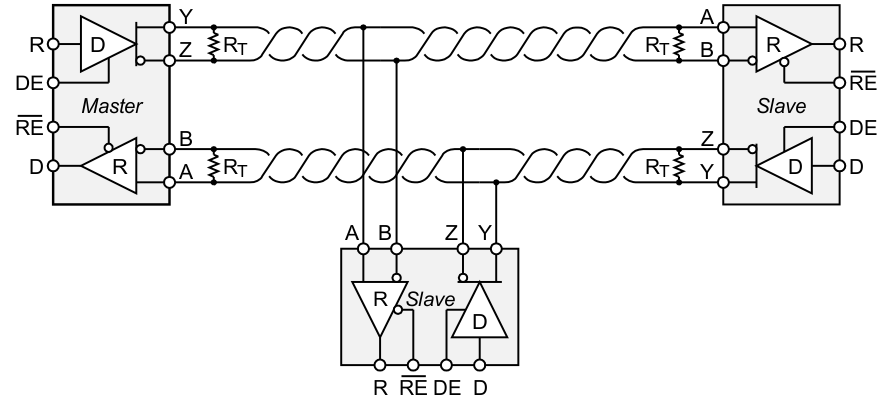
Each driver and receiver has separate input and output pins for full-duplex bus communication designs. They are designed for RS-422 and RS-485 data transmission over cable lengths of up to 1500 meters.
The SN65HVD30, SN65HVD31, and SN65HVD32 devices are fully enabled with no external enabling pins.
The SN65HVD33, SN65HVD34, and SN65HVD35 devices have active-high driver enables and active-low receiver enables. A low, less than 1 μA, standby current can be achieved by disabling both the driver and receiver.
All devices are characterized for ambient temperatures from –40°C to 85°C. Low power dissipation allows operation at temperatures up to 105°C or 125°C, depending on package option.
| PART NUMBER | PACKAGE | BODY SIZE (NOM) |
|---|---|---|
| SN65HVD30 | SOIC (8) | 4.90 mm × 3.91 mm |
| SN65HVD31 | ||
| SN65HVD32 | ||
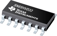
| SN65HVD33 | SOIC (14) | 8.65 mm × 3.91 mm |
| VQFN (20) | 4.50 mm × 3.50 mm | |
| SN65HVD34 | SOIC (14) | 8.65 mm × 3.91 mm |
| SN65HVD35 |


