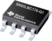

SN65LBC176-Q1是TI公司的一款无产品,SN65LBC176-Q1是汽车类差动总线接收器,本页介绍了SN65LBC176-Q1的产品说明、应用、特性等,并给出了与SN65LBC176-Q1相关的TI元器件型号供参考。
SN65LBC176-Q1 - 汽车类差动总线接收器 - 无 - RS-485收发器 - TI公司(Texas Instruments,德州仪器)
The SN65LBC176 differential bus transceiver is a monolithic, integrated circuit designed for bidirectional data communication on multipoint bus-transmission lines. It is designed for balanced transmission lines and meets ANSI Standard RS-485 and ISO 8482:1987(E).
The SN65LBC176 combines a 3-state, differential line driver and a differential input line receiver, both of which operate from a single 5-V power supply. The driver and receiver have active-high and active-low enables, respectively, which can externally connect together to function as a direction control. The driver differential outputs and the receiver differential inputs connect internally to form a differential input/output (I/O) bus port that is designed to offer minimum loading to the bus whenever the driver is disabled or VCC = 0. This port features wide positive and negative common-mode voltage ranges, making the device suitable for party-line applications. Very low device supply current can be achieved by disabling the driver and the receiver. Both the driver and receiver are available as cells in the Texas Instruments LinASIC™ Library.
This transceiver is suitable for ANSI Standard RS-485 and ISO 8482:1987 (E) applications to the extent that they are specified in the operating conditions and characteristics section of this data sheet. Certain limits contained in the ANSI Standard RS-485 and ISO 8482:1987 (E) are not met or cannot be tested over the entire extended temperature range.
- Qualified for Automotive Applications
- Bidirectional Transceiver
- Meet or Exceed the Requirements of ANSI Standard RS-485 and ISO 8482:1987(E)
- High-Speed Low-Power LinBiCMOS™ Circuitry
- Designed for High-Speed Operation in Both Serial and Parallel Applications
- Low Skew
- Designed for Multipoint Transmission on Long Bus Lines in Noisy Environments
- Very Low Disabled Supply-Current Requirements . . . 200 µA Maximum
- Wide Positive and Negative Input/Output Bus Voltage Ranges
- Driver Output Capacity . . . ±60 mA
- Thermal-Shutdown Protection
- Driver Positive-and Negative-Current Limiting
- Open-Circuit Fail-Safe Receiver Design
- Receiver Input Sensitivity . . . ±200 mV Max
- Receiver Input Hysteresis . . . 50 mV Typ
- Operate From a Single 5-V Supply
- Glitch-Free Power-Up and Power-Down Protection
LinBiCMOS and LinASIC are trademarks of Texas Instruments Incorporated.


