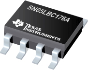

SN65LBC176A是TI公司的一款无产品,SN65LBC176A是差动总线收发器,本页介绍了SN65LBC176A的产品说明、应用、特性等,并给出了与SN65LBC176A相关的TI元器件型号供参考。
SN65LBC176A - 差动总线收发器 - 无 - RS-485收发器 - TI公司(Texas Instruments,德州仪器)
The SN65LBC176A, SN65LBC176AQ, and SN75LBC176A differential bus transceivers are monolithic, integrated circuits designed for bidirectional data communication on multipoint bus-transmission lines. They are designed for balanced transmission lines and are compatible with ANSI standard TIA/EIA-485-A and ISO 8482. The A version offers improved switching performance over its predecessors without sacrificing significantly more power.
The SN65LBC176A, SN65LBC176AQ, and SN75LBC176A combine a 3-state, differential line driver and a differential input line receiver, both of which operate from a single 5-V power supply. The driver and receiver have active-high and active-low enables, respectively, which can externally connect together to function as a direction control. The driver differential outputs and the receiver differential inputs connect internally to form a differential input/output (I/O) bus port that is designed to offer minimum loading to the bus whenever the driver is disabled or VCC = 0. This port features wide positive and negative common-mode voltage ranges, making the device suitable for party-line applications. Very low device supply current can be achieved by disabling the driver and the receiver.
- Designed for Signal Rates Up to 30 Mbps
- Bus-Pin ESD Protection Exceeds 12 kV HBM
- Compatible With ANSI Standard TIA/EIA-485-A and ISO 8482:1987(E)
- Low Skew
- Designed for Multipoint Transmission on Long Bus Lines in Noisy Environments
- Very Low Disabled Supply-Current Requirements...700 µA Maximum
- Common Mode Voltage Range of -7 V to 12 V
- Thermal-Shutdown Protection
- Driver Positive and Negative Current Limiting
- Open-Circuit Fail-Safe Receiver Design
- Receiver Input Sensitivity...±200 mV Max
- Receiver Input Hysteresis...50 mV Typ
- Glitch-Free Power-Up and Power-Down Protection
- Available in Q-Temp Automotive High Reliability Automotive Applications Configuration Control / Print Support Qualification to Automotive Standards
LinBiCMOS and LinASIC are trademarks of Texas Instruments. Signaling rate by TIA/EIA-485-A definition restrict transition times to 30% of the bit length, and much higher signaling rates may be achieved without this requirement as displayed in the TYPICAL CHARACTERISTICS of this device.


