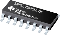

SN65LVDM050-Q1是TI公司的一款多点LVDS(MLVDS/BLVDS/LVDM)产品,SN65LVDM050-Q1是汽车类双路 LVDS 发送器/接收器,本页介绍了SN65LVDM050-Q1的产品说明、应用、特性等,并给出了与SN65LVDM050-Q1相关的TI元器件型号供参考。
SN65LVDM050-Q1 - 汽车类双路 LVDS 发送器/接收器 - 多点LVDS(MLVDS/BLVDS/LVDM) - LVDS/M-LVDS/ECL/CML - TI公司(Texas Instruments,德州仪器)
The SN65LVDM050, and SN65LVDM051 are differential line drivers and receivers that use low-voltage differential signaling (LVDS) to achieve signaling rates as high as 500 Mbps (per TIA/EIA-644 definition). These circuits are similar to TIA/EIA-644 standard compliant devices (SN65LVDS) counterparts, except that the output current of the drivers is doubled. This modification provides a minimum differential output voltage magnitude of 247 mV across a 50- load simulating two transmission lines in parallel. This allows having data buses with more than one driver or with two line termination resistors. The receivers detect a voltage difference of 50 mV with up to 1 V of ground potential difference between a transmitter and receiver.
The intended application of these devices and signaling techniques is point-to-point and multipoint, baseband data transmission over a controlled impedance media of approximately 100 of characteristic impedance. The transmission media may be printed-circuit board traces, backplanes, or cables.
The SN65LVDM050Q and SN65LVDM051Q are characterized for operation from –40°C to 125°C. Additionally, Q1 suffixed parts are qualified in accordance with AEC-Q100 stress test qualification for integrated circuits.
- Qualified for Automotive Applications
- ESD Protection Exceeds 2000 V Per MIL-STD-883, Method 3015; Exceeds 200 V Using Machine Model (C = 200 pF, R = 0)
- Low-Voltage Differential 50- Line Drivers and Receivers
- Signaling Rates up to 500 Mbps
- Bus-Terminal ESD Exceeds 12 kV
- Operates From a Single 3.3 V Supply
- Low-Voltage Differential Signaling With Typical Output Voltages of 340 mV With a 50- Load
- Valid Output With as Little as 50-mV Input Voltage Difference
- Propagation Delay Times
- Driver: 1.7 ns Typ
- Receiver: 3.7 ns Typ
- Power Dissipation at 200 MHz
- Driver: 50 mW Typical
- Receiver: 60 mW Typical
- LVTTL Input Levels Are 5 V Tolerant
- Driver Is High Impedance When Disabled or With VCC < 1.5 V
- Receiver Has Open-Circuit Fail Safe


