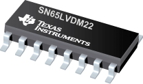

SN65LVDM22是TI公司的一款多点LVDS(MLVDS/BLVDS/LVDM)产品,SN65LVDM22是双路多路复用 LVDM 中继器,本页介绍了SN65LVDM22的产品说明、应用、特性等,并给出了与SN65LVDM22相关的TI元器件型号供参考。
SN65LVDM22 - 双路多路复用 LVDM 中继器 - 多点LVDS(MLVDS/BLVDS/LVDM) - LVDS/M-LVDS/ECL/CML - TI公司(Texas Instruments,德州仪器)
The SN65LVDS22 and SN65LVDM22 are differential line drivers and receivers that use low-voltage differential signaling (LVDS) to achieve signaling rates as high as 400 Mbps. The receiver outputs can be switched to either or both drivers through the multiplexer control signals S0 and S1. This allows the flexibility to perform splitter or signal routing functions with a single device.
The TIA/EIA-644 standard compliant electrical interface provides a minimum differential output voltage magnitude of 247 mV into a 100- load.
The intended application of these devices and signaling technique is for both point-to-point baseband (single termination) and multipoint (double termination) data transmissions over controlled impedance media. The transmission media may be printed-circuit board traces, backplanes, or cables. (Note: The ultimate rate and distance of data transfer is dependent upon the attenuation characteristics of the media, the noise coupling to the environment, and other application specific characteristics).
The SN65LVDS22 and SN65LVDM22 are characterized for operation from –40°C to 85°C.
- Meets or Exceeds the Requirements of ANSI TIA/EIA-644-1995 Standard
- Designed for Clock Rates up to 200 MHz (400 Mbps)
- Designed for Data Rates up to 250 Mbps
- Pin Compatible With SN65LVDS122 and SN65LVDT122, 1.5 Gbps 2x2 Crosspoint Switch From TI
- ESD Protection Exceeds 12 kV on Bus Pins
- Operates From a Single 3.3-V Supply
- Low-Voltage Differential Signaling With Output Voltages of 350 mV Into:
- 100- Load (SN65LVDS22)
- 50- Load (SN65LVDM22)
- Propagation Delay Time; 4 ns Typ
- Power Dissipation at 400 Mbps of 150 mW
- Bus Pins Are High Impedance When Disabled or With VCC Less Than 1.5 V
- LVTTL Levels Are 5 V Tolerant
- Open-Circuit Fail Safe Receiver


