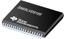

SN65LVDS109是TI公司的一款LVDSPHY(<800Mbps)产品,SN65LVDS109是双路 4 端口 LVDS 中继器,本页介绍了SN65LVDS109的产品说明、应用、特性等,并给出了与SN65LVDS109相关的TI元器件型号供参考。
SN65LVDS109 - 双路 4 端口 LVDS 中继器 - LVDSPHY(<800Mbps) - LVDS/M-LVDS/ECL/CML - TI公司(Texas Instruments,德州仪器)
The SN65LVDS109 and SN65LVDS117 are configured as two identical banks, each bank having one differential line receiver connected to either four ('109) or eight ('117) differential line drivers. The outputs are arranged in pairs having one output from each of the two banks. Individual output enables are provided for each pair of outputs and an additional enable is provided for all outputs.
The line receivers and line drivers implement the electrical characteristics of low-voltage differential signaling (LVDS). LVDS, as specified in EIA/TIA-644, is a data signaling technique that offers low power, low noise emission, high noise immunity, and high switching speeds. (Note: The ultimate rate and distance of data transfer is dependent upon the attenuation characteristics of the media, the noise coupling to the environment, and other system characteristics.)
The intended application of these devices, and the LVDS signaling technique, is for point-to-point or point-to-multipoint (distributed simplex) baseband data transmission on controlled impedance media of approximately 100 . The transmission media may be printed-circuit board traces, backplanes, or cables. The large number of drivers integrated into the same silicon substrate, along with the low pulse skew of balanced signaling, provides extremely precise timing alignment of the signals being repeated from the inputs. This is particularly advantageous for implementing system clock and data distribution trees.
The SN65LVDS109 and SN65LVDS117 are characterized for operation from –40°C to 85°C.
- Two Line Receivers and Eight ('109) or Sixteen ('117) Line Drivers Meet or Exceed the Requirements of ANSI EIA/TIA-644 Standard
- Typical Data Signaling Rates to 400 Mbps or Clock Frequencies to 400 MHz
- Outputs Arranged in Pairs From Each Bank
- Enabling Logic Allows Individual Control of Each Driver Output Pair, Plus All Outputs
- Low-Voltage Differential Signaling With Typical Output Voltage of 350 mV and a 100- Load
- Electrically Compatible With LVDS, PECL, LVPECL, LVTTL, LVCMOS, GTL, BTL, CTT, SSTL, or HSTL Outputs With External Termination Networks
- Propagation Delay Times < 4.5 ns
- Output Skew Less Than 550 psBank Skew Less Than150 ps Part-to-Part Skew Less Than 1.5 ns
- Total Power Dissipation Typically <500 mW With All Ports Enabled and at 200 MHz
- Driver Outputs or Receiver Input Equals High Impedance When Disabled or With
下面可能是您感兴趣的TI公司LVDSPHY(<800Mbps)元器件
- BQ77PL900 - 5 至 10 节锂离子电池保护和 AFE
- LP2950-50 - Fixed 5V Micropower Voltage Regulator with Shutdown
- LMZ31710 - 采用 QFN 封装具有 2.95V-17V 输入及均流功能的 10A SIMPLE SWITCHER? 电源模块
- UC3714 - 辅助开关 FET 驱动器
- CDCV304-EP - 通用和 PCI-X 1:4 时钟缓冲器
- LM8365 - 具有可编程输出延迟的微功耗欠压感应电路
- LM3248 - 具有 ACB 的 LM3248 2.7MHz、2.5A 可调节升压-降压 DC-DC 转换器
- LM22679 - 具有可调节软启动和电流限制的 5A SIMPLE SWITCHER,降压电压稳压器
- MAX211 - 具有 ?15kV ESD 保护的 5V 多通道 RS-232 线路驱动器/接收器
- MSP430F5522 - MSP430F551x、MSP430F552x 混合信号微处理器


