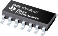

SN65LVDS180-Q1是TI公司的一款LVDSPHY(<800Mbps)产品,SN65LVDS180-Q1是汽车类高速差动线路驱动器和接收器,本页介绍了SN65LVDS180-Q1的产品说明、应用、特性等,并给出了与SN65LVDS180-Q1相关的TI元器件型号供参考。
SN65LVDS180-Q1 - 汽车类高速差动线路驱动器和接收器 - LVDSPHY(<800Mbps) - LVDS/M-LVDS/ECL/CML - TI公司(Texas Instruments,德州仪器)
The SN65LVDS180, SN65LVDS050, and SN65LVDS051 are differential line drivers and receivers that use low-voltage differential signaling (LVDS) to achieve signaling rates as high as 400 Mbps. The TIA/EIA-644 standard compliant electrical interface provides a minimum differential output voltage magnitude of 247 mV into a 100-Ω load and receipt of 50-mV signals with up to 1 V of ground potential difference between a transmitter and receiver.
The intended application of this device and signaling technique is for point-to-point baseband data transmission over controlled impedance media of approximately 100-Ω characteristic impedance. The transmission media may be printed-circuit board traces, backplanes, or cables. (Note: The ultimate rate and distance of data transfer is dependent upon the attenuation characteristics of the media, the noise coupling to the environment, and other application specific characteristics).
The devices offer various driver, receiver, and enabling combinations in industry standard footprints. Since these devices are intended for use in simplex or distributed simplex bus structures, the driver enable function does not put the differential outputs into a high-impedance state but rather disconnects the input and reduces the quiescent power used by the device. (For these functions with a high-impedance driver output, see the SN65LVDM series of devices.) All devices are characterized for operation from −40°C to 85°C.
- Qualified for Automotive Applications
- ESD Protection Exceeds 2000 V Per MIL-STD-883, Method 3015; Exceeds 200 V Using Machine Model (C = 200 pF, R = 0)
- Meets or Exceeds the Requirements of ANSI TIA/EIA-644-1995 Standard
- Signaling Rates up to 400 Mbps
- Bus-Terminal ESD Exceeds 12 kV
- Operates From a Single 3.3-V Supply
- Low-Voltage Differential Signaling With Typical Output Voltages of 350 mV and a 100-Ω Load
- Propagation Delay Times
- Driver: 1.7 ns Typ
- Receiver: 3.7 ns Typ
- Power Dissipation at 200 MHz
- Driver: 25 mW Typical
- Receiver: 60 mW Typical
- LVTTL Input Levels Are 5-V Tolerant
- Receiver Maintains High Input Impedance With VCC < 1.5 V
- Receiver Has Open-Circuit Fail Safe


