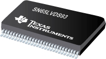

SN65LVDS93是TI公司的一款BLVDS/LVDS串行器/解串器(<100MHz)产品,SN65LVDS93是Serdes(串行器/解串器)发送器,本页介绍了SN65LVDS93的产品说明、应用、特性等,并给出了与SN65LVDS93相关的TI元器件型号供参考。
SN65LVDS93 - Serdes(串行器/解串器)发送器 - BLVDS/LVDS串行器/解串器(<100MHz) - 串行器、解串器 - TI公司(Texas Instruments,德州仪器)
The SN65LVDS93 LVDS serdes (serializer/ deserializer) transmitter contains four 7-bit parallel- load serial-out shift registers, a 7× clock synthesizer, and five low-voltage differential signaling (LVDS) drivers in a single integrated circuit. These functions allow 28 bits of single-ended LVTTL data to be synchronously transmitted over five balanced-pair conductors for receipt by a compatible receiver, such as the SN65LVDS94.
When transmitting, data bits D0 through D27 are each loaded into registers upon the edge of the input clock signal (CLKIN). The rising or falling edge of the clock can be selected via the clock select (CLKSEL) pin. The frequency of CLKIN is multiplied seven times and then used to serially unload the data registers in 7-bit slices. The four serial streams and a phase-locked clock (CLKOUT) are then output to LVDS output drivers. The frequency of CLKOUT is the same as the input clock, CLKIN.
The SN65LVDS93 requires no external components and little or no control. The data bus appears the same at the input to the transmitter and output of the receiver with the data transmission transparent to the user(s). The only user intervention is selecting a clock rising edge by inputting a high level to CLKSEL or a falling edge with a low-level input and the possible use of the shutdown/clear (SHTDN). SHTDN is an active-low input to inhibit the clock and shut off the LVDS output drivers for lower power consumption. A low level on this signal clears all internal registers at a low level.
The SN65LVDS93 is characterized for operation over ambient air temperatures of -40°C to 85°C.
- 28:4 Data Channel Compression at up to 1.904 Gigabits per Second Throughput
- Suited for Point-to-Point Subsystem Communication With Very Low EMI
- 28 Data Channels Plus Clock in Low-Voltage TTL and 4 Data Channels Plus Clock Out Low-Voltage Differential
- Selectable Rising or Falling Clock Edge Triggered Inputs
- Bus Pins Tolerate 6-kV HBM ESD
- Operates From a Single 3.3-V Supply and 250 mW (Typ)
- 5-V Tolerant Data Inputs
- Packaged in Thin Shrink Small-Outline Package With 20 Mil Terminal Pitch
- Consumes <1 mW When Disabled
- Wide Phase-Lock Input Frequency Range 20 MHz to 68 MHz
- No External Components Required for PLL
- Outputs Meet or Exceed the Requirements of ANSI EIA/TIA-644 Standard
- Industrial Temperature Qualified TA = -40°C to 85°C
- Replacement for the DS90CR285


