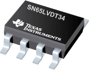

SN65LVDT34是TI公司的一款LVDSPHY(<800Mbps)产品,SN65LVDT34是具有 -4 至 5V 共模范围的双路 LVDS 接收器,本页介绍了SN65LVDT34的产品说明、应用、特性等,并给出了与SN65LVDT34相关的TI元器件型号供参考。
SN65LVDT34 - 具有 -4 至 5V 共模范围的双路 LVDS 接收器 - LVDSPHY(<800Mbps) - LVDS/M-LVDS/ECL/CML - TI公司(Texas Instruments,德州仪器)
This family of four LVDS data line receivers offers the widest common-mode input voltage range in the industry. These receivers provide an input voltage range specification compatible with a 5-V PECL signal as well as an overall increased ground-noise tolerance. They are in industry standard footprints with integrated termination as an option.
Precise control of the differential input voltage thresholds allows for inclusion of 50 mV of input voltage hysteresis to improve noise rejection on slowly changing input signals. The input thresholds are still no more than ±50 mV over the full input common-mode voltage range.
The high-speed switching of LVDS signals usually necessitates the use of a line impedance matching resistor at the receiving-end of the cable or transmission media. The SN65LVDT series of receivers eliminates this external resistor by integrating it with the receiver. The nonterminated SN65LVDS series is also available for multidrop or other termination circuits.
The receivers can withstand ±15 kV human-body model (HBM) and ±600 V machine model (MM) electrostatic discharges to the receiver input pins with respect to ground without damage. This provides reliability in cabled and other connections where potentially damaging noise is always a threat.
The receivers also include a (patent pending) failsafe circuit that will provide a high-level output within 600 ns after loss of the input signal. The most common causes of signal loss are disconnected cables, shorted lines, or powered-down transmitters. The failsafe circuit prevents noise from being received as valid data under these fault conditions. This feature may also be used for Wired-Or bus signaling. See The Active Failsafe Feature of the SN65LVDS32B application note.
The intended application and signaling technique of these devices is point-to-point baseband data transmission over controlled impedance media of approximately 100 . The transmission media may be printed-circuit board traces, backplanes, or cables. The ultimate rate and distance of data transfer is dependent upon the attenuation characteristics of the media and the noise coupling to the environment.
The SN65LVDS33, SN65LVDT33, SN65LVDS34 and SN65LVDT34 are characterized for operation from –40°C to 85°C.
- 400-Mbps Signaling Rate1 and 200-Mxfr/s Data Transfer Rate
- Operates With a Single 3.3-V Supply
- –4-V to 5-V Common-Mode Input Voltage Range
- Differential Input Thresholds <±50 mV With 50 mV of Hysteresis Over Entire Common-Mode Input Voltage Range
- Integrated 110- Line Termination Resistors On LVDT Products
- TSSOP Packaging (33 Only)
- Complies With TIA/EIA-644 (LVDS)
- Active Failsafe Assures a High-Level Output With No Input
- Bus-Pin ESD Protection Exceeds 15 kV HBM
- Input Remains High-Impedance on Power Down
- TTL Inputs Are 5-V Tolerant
- Pin-Compatible With the AM26LS32, SN65LVDS32B, µA9637, SN65LVDS9637B
1 The signaling rate of a line, is the number of voltage transitions that are made per second expressed in the units bps (bits per second).


