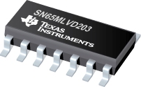

SN65MLVD203是TI公司的一款多点LVDS(MLVDS/BLVDS/LVDM)产品,SN65MLVD203是全双工 M-LVDS 收发器,本页介绍了SN65MLVD203的产品说明、应用、特性等,并给出了与SN65MLVD203相关的TI元器件型号供参考。
SN65MLVD203 - 全双工 M-LVDS 收发器 - 多点LVDS(MLVDS/BLVDS/LVDM) - LVDS/M-LVDS/ECL/CML - TI公司(Texas Instruments,德州仪器)
The SN65MLVD201, 203, 206, and 207 are multipoint-low-voltage differential (M-LVDS) line drivers and receivers, which are optimized to operate at signaling rates up to 200 Mbps. All parts comply with the multipoint low-voltage differential signaling (M-LVDS) standard TIA/EIA-899. These circuits are similar to their TIA/EIA-644 standard compliant LVDS counterparts, with added features to address multipoint applications. The driver output has been designed to support multipoint buses presenting loads as low as 30 , and incorporates controlled transition times to allow for stubs off of the backbone transmission line.
These devices have Type-1 and Type-2 receivers that detect the bus state with as little as 50 mV of differential input voltage over a common-mode voltage range of –1 V to 3.4 V. The Type-1 receivers exhibit 25 mV of differential input voltage hysteresis to prevent output oscillations with slowly changing signals or loss of input. Type-2 receivers include an offset threshold to provide a known output state under open-circuit, idle-bus, and other faults conditions. The devices are characterized for operation from –40°C to 85°C.
- Low-Voltage Differential 30- Line Drivers and Receivers for Signaling Rates(1) Up to 200 Mbps
- Type-1 Receivers Incorporate 25 mV of Hysteresis
- Type-2 Receivers Provide an Offset (100 mV) Threshold to Detect Open-Circuit and Idle-Bus Conditions
- Meets or Exceeds the M-LVDS Standard TIA/EIA-899 for Multipoint Data Interchange
- Controlled Driver Output Voltage Transition Times for Improved Signal Quality
- –1 V to 3.4 V Common-Mode Voltage Range Allows Data Transfer With 2 V of Ground Noise
- Bus Pins High Impedance When Disabled or VCC ≤ 1.5 V
- 100-Mbps Devices Available (SN65MLVD200A, 202A, 204A, 205A)
- M-LVDS Bus Power Up/Down Glitch Free
- APPLICATIONS
- Low-Power High-Speed Short-Reach Alternative to TIA/EIA-485
- Backplane or Cabled Multipoint Data and Clock Transmission
- Cellular Base Stations
- Central-Office Switches
- Network Switches and Routers
(1) The signaling rate of a line, is the number of voltage transitions that are made per second expressed in the units bps (bits per second).


