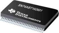

SN74ABT162601是TI公司的一款通用总线收发器(UBT)产品,SN74ABT162601是具有三态输出的 18 位通用总线收发器,本页介绍了SN74ABT162601的产品说明、应用、特性等,并给出了与SN74ABT162601相关的TI元器件型号供参考。
SN74ABT162601 - 具有三态输出的 18 位通用总线收发器 - 通用总线收发器(UBT) - 通用总线功能 - TI公司(Texas Instruments,德州仪器)
These 18-bit universal bus transceivers combine D-type latches and D-type flip-flops to allow data flow in transparent, latched, and clocked modes.
Data flow in each direction is controlled by output-enable (OEAB\ and OEBA\), latch-enable (LEAB and LEBA), and clock (CLKAB and CLKBA) inputs. The clock can be controlled by the clock-enable (CLKENAB\ and CLKENBA\) inputs.
For A-to-B data flow, the device operates in the transparent mode when LEAB is high. When LEAB is low, the A data is latched if CLKAB is held at a high or low logic level. If LEAB is low, the A data is stored in the latch/flip-flop on the low-to-high transition of CLKAB. Output-enable OEAB\ is active-low. When OEAB\ is low, the outputs are active. When OEAB\ is high, the outputs are in the high-impedance state. Data flow for B to A is similar to that of A to B but uses OEBA\, LEBA, CLKBA, and CLKENBA\.
The B-port outputs, which are designed to source or sink up to 12 mA, include equivalent 25- series resistors to reduce overshoot and undershoot.
When VCC is between 0 and 2.1 V, the device is in the high-impedance state during power up or power down. However, to ensure the high-impedance state above 2.1 V, OE\ should be tied to VCC through a pullup resistor; the minimum value of the resistor is determined by the current-sinking capability of the driver.
The SN54ABT162601 is characterized for operation over the full military temperature range of -55°C to 125°C. The SN74ABT162601 is characterized for operation from -40°C to 85°C.
- Members of the Texas Instruments WidebusTM Family
- B-Port Outputs Have Equivalent 25- Series Resistors, So No External Resistors Are Required
- State-of-the-Art EPIC-II BTM BiCMOS Design Significantly Reduces Power Dissipation
- UBTTM (Universal Bus Transceiver) Combines D-Type Latches and D-Type Flip-Flops for Operation in Transparent, Latched, Clocked, or Clock-Enabled Mode
- Latch-Up Performance Exceeds 500 mA Per JESD 17
- Typical VOLP (Output Ground Bounce) < 0.8 V at VCC = 5 V, TA = 25°C
- High-Impedance State During Power Up and Power Down
- Flow-Through Architecture Optimizes PCB Layout
- Package Options Include Plastic 300-mil Shrink Small-Outline (DL) and Thin Shrink Small-Outline (DGG) Packages and 380-mil Fine-Pitch Ceramic Flat (WD) Package Using 25-mil Center-to-Center Spacings
Widebus, EPIC-IIB, and UBT are trademarks of Texas Instruments Incorporated.


