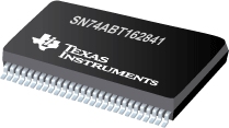

SN74ABT162841是TI公司的一款D类锁存器产品,SN74ABT162841是具有三态输出的 20 位总线接口 D 类锁存器,本页介绍了SN74ABT162841的产品说明、应用、特性等,并给出了与SN74ABT162841相关的TI元器件型号供参考。
SN74ABT162841 - 具有三态输出的 20 位总线接口 D 类锁存器 - D类锁存器 - 触发器/锁存器/寄存器 - TI公司(Texas Instruments,德州仪器)
These 20-bit transparent D-type latches feature noninverting 3-state outputs designed specifically for driving highly capacitive or relatively low-impedance loads. They are particularly suitable for implementing buffer registers, I/O ports, bidirectional bus drivers, and working registers.
The ’ABT162841 devices can be used as two 10-bit latches or one 20-bit latch. While the latch-enable (1LE or 2LE) input is high, the Q outputs of the corresponding 10-bit latch follow the data (D) inputs. When LE is taken low, the Q outputs are latched at the levels set up at the D inputs.
A buffered output-enable (1OE\ or 2OE\) input can be used to place the outputs of the corresponding 10-bit latch in either a normal logic state (high or low logic levels) or a high-impedance state. In the high-impedance state, the outputs neither load nor drive the bus lines significantly.
The outputs, which are designed to sink up to 12 mA, include equivalent 25- series resistors to reduce overshoot and undershoot.
These devices are fully specified for hot-insertion applications using Ioff and power-up 3-state. The Ioff circuitry disables the outputs, preventing damaging current backflow through the devices when they are powered down. The power-up 3-state circuitry places the outputs in the high-impedance state during power up and power down, which prevents driver conflict.
To ensure the high-impedance state during power up or power down, OE\ shall be tied to VCC through a pullup resistor; the minimum value of the resistor is determined by the current-sinking capability of the driver.
OE\ does not affect the internal operation of the latches. Old data can be retained or new data can be entered while the outputs are in the high-impedance state.
- Members of the Texas Instruments Widebus™ Family
- Output Ports Have Equivalent 25- Series Resistors, So No External Resistors Are Required
- Typical VOLP (Output Ground Bounce) <0.8 V at VCC = 5 V, TA = 25°C
- High-Impedance State During Power Up and Power Down
- Ioff and Power-Up 3-State Support Hot Insertion
- Distributed VCC and GND Pins Minimize High-Speed Switching Noise
- Flow-Through Architecture Optimizes PCB Layout
- Latch-Up Performance Exceeds 500 mA Per JEDEC Standard JESD-17
Widebus is a trademark of Texas Instruments.


