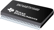

SN74ABTH16460是TI公司的一款解码器/编码器/多路复用器产品,SN74ABTH16460是具有三态输出的 4 至 1 多路复用器/多路解复用器收发器,本页介绍了SN74ABTH16460的产品说明、应用、特性等,并给出了与SN74ABTH16460相关的TI元器件型号供参考。
SN74ABTH16460 - 具有三态输出的 4 至 1 多路复用器/多路解复用器收发器 - 解码器/编码器/多路复用器 - 特殊逻辑 - TI公司(Texas Instruments,德州仪器)
The 'ABTH16460 are 4-bit to 1-bit multiplexed registered transceivers used in applications where four separate data paths must be multiplexed onto or demultiplexed from a single data path. Typical applications include multiplexing and/or demultiplexing of address and data information in microprocessor or bus-interface applications. These devices also are useful in memory-interleaving applications.
Five 4-bit I/O ports (1A-4A, 1B1-4, 2B1-4, 3B1-4, and 4B1-4) are available for address and/or data transfer. The output-enable (OEB\, OEB1\-OEB4\, and OEA\) inputs control the bus-transceiver functions. These control signals also allow 4-bit or 16-bit control, depending on the OEB\ level.
Address and/or data information can be stored using the internal storage latches/flip-flops. The latch-enable (LEB1-LEB4, LEBA, and LEAB1-LEAB4) and clock/clock-enable (CLK/CLKEN\) inputs are used to control data storage. When either one of the latch-enable inputs is high, the latch is transparent (clock is a don't care as long as the latch enable is high). When the latch-enable input goes low (providing that the clock does not transit from low to high), the data present at the inputs is latched and remains latched until the latch-enable input is returned high. When the clock enable is low and the corresponding latch enable is low, data can be clocked on the low-to-high transition of the clock. When either the clock enable or the corresponding latch enable is high, the clock is a don't care.
Four select pins (SEL0, SEL1, CE_SEL0, and CE_SEL1) are provided to multiplex data (A port), or to select one of four clock enables (B port). This allows the user the flexibility of controlling one bit at a time.
Active bus-hold circuitry is provided to hold unused or floating data inputs at a valid logic level.
When VCC is between 0 and 2.1 V, the device is in the high-impedance state during power up or power down. However, to ensure the high-impedance state above 2.1 V, OE\ should be tied to VCC through a pullup resistor; the minimum value of the resistor is determined by the current-sinking capability of the driver.
The SN54ABTH16460 is characterized for operation over the full military temperature range of -55°C to 125°C. The SN74ABTH16460 is characterized for operation from -40°C to 85°C.
- Members of the Texas Instruments WidebusTM Family
- State-of-the-Art EPIC-II BTM BiCMOS Design Significantly Reduces Power Dissipation
- Latch-Up Performance Exceeds 500 mA Per JEDEC Standard JESD-17
- Typical VOLP (Output Ground Bounce) < 1 V at VCC = 5 V, TA = 25°C
- High-Impedance State During Power Up and Power Down
- Distributed VCC and GND Pin Configuration Minimizes High-Speed Switching Noise
- Flow-Through Architecture Optimizes PCB Layout
- High-Drive Outputs (-32-mA IOH, 64-mA IOL)
- Bus Hold on Data Inputs Eliminates the Need for External Pullup/Pulldown Resistors
- Package Options Include Plastic 300-mil Shrink Small-Outline (DL) and Thin Shrink Small-Outline (DGG) Packages and 380-mil Fine-Pitch Ceramic Flat (WD) Package Using 25-mil Center-to-Center Spacings
Widebus and EPIC-IIB are trademarks of Texas Instruments Incorporated.


