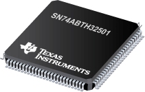

SN74ABTH32501是TI公司的一款通用总线收发器(UBT)产品,SN74ABTH32501是具有三态输出的 36 位通用总线收发器,本页介绍了SN74ABTH32501的产品说明、应用、特性等,并给出了与SN74ABTH32501相关的TI元器件型号供参考。
SN74ABTH32501 - 具有三态输出的 36 位通用总线收发器 - 通用总线收发器(UBT) - 通用总线功能 - TI公司(Texas Instruments,德州仪器)
These 36-bit UBTs combine D-type latches and D-type flip-flops to allow data flow in transparent, latched, and clocked modes.
Data flow in each direction is controlled by output-enable (OEAB and OEBA\), latch-enable (LEAB and LEBA), and clock (CLKAB and CLKBA) inputs. For A-to-B data flow, the device operates in the transparent mode when LEAB is high. When LEAB is low, the A data is latched if CLKAB is held at a high or low logic level. If LEAB is low, the A data is stored in the latch/flip-flop on the low-to-high transition of CLKAB. Data flow for B to A is similar to that of A to B, but uses OEBA\, LEBA, and CLKBA.
Output-enable OEAB is active high. When OEAB is high, the outputs are active. When OEAB is low, the outputs are in the high-impedance state. The output enables are complementary (OEAB is active high, and OEBA\ is active low).
When VCC is between 0 and 2.1 V, the device is in the high-impedance state during power up or power down. However, to ensure the high-impedance state above 2.1 V, OE\ should be tied to VCC through a pullup resistor and OE should be tied to GND through a pulldown resistor; the minimum value of the resistor is determined by the current-sinking/current-sourcing capability of the driver.
Active bus-hold circuitry is provided to hold unused or floating data inputs at a valid logic level.
The SN54ABTH32501 is characterized for operation over the full military temperature range of -55°C to 125°C. The SN74ABTH32501 is characterized for operation from -40°C to 85°C
- Members of the Texas Instruments Widebus+TM Family
- State-of-the-Art EPIC-II BTM BiCMOS Design Significantly Reduces Power Dissipation
- UBTTM (Universal Bus Transceiver) Combines D-Type Latches and D-Type Flip-Flops for Operation in Transparent, Latched, or Clocked Mode
- ESD Protection Exceeds 2000 V Per MIL-STD-883, Method 3015; Exceeds 200 V Using Machine Model (C = 200 pF, R = 0)
- Latch-Up Performance Exceeds 500 mA Per JEDEC Standard JESD-17
- Released as DSCC SMD 5962-9557601NXD
- Typical VOLP (Output Ground Bounce) < 0.8 V at VCC = 5 V, TA = 25°C
- High-Impedance State During Power Up and Power Down
- Distributed VCC and GND Pin Configuration Minimizes High-Speed Switching Noise
- High-Drive Outputs (-32-mA IOH, 64-mA IOL)
- Bus Hold on Data Inputs Eliminates the Need for External Pullup/Pulldown Resistors
- Package Options Include 100-Pin Plastic Thin Quad Flat (PZ) Package With 14 × 14-mm Body Using 0.5-mm Lead Pitch and Space-Saving 100-Pin Ceramic Quad Flat (HS) Package
Widebus+, EPIC-IIB, and UBT are trademarks of Texas Instruments Incorporated.
The HS package is not production released.


