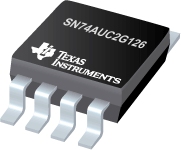

SN74AUC2G126是TI公司的一款无产品,SN74AUC2G126是具有三态输出的双总线缓冲器闸,本页介绍了SN74AUC2G126的产品说明、应用、特性等,并给出了与SN74AUC2G126相关的TI元器件型号供参考。
SN74AUC2G126 - 具有三态输出的双总线缓冲器闸 - 无 - 小尺寸逻辑器件 - TI公司(Texas Instruments,德州仪器)
- Available in the Texas Instruments NanoFree™ Package
- Optimized for 1.8-V Operation and Is 3.6-V I/O Tolerant to Support Mixed-Mode Signal Operation
- Ioff Supports Partial-Power-Down Mode Operation
- Sub-1-V Operable
- Max tpd of 1.9 ns at 1.8 V
- Low Power Consumption, 10 µA at 1.8 V
- ±8-mA Output Drive at 1.8 V
- Latch-Up Performance Exceeds 100 mA Per JESD 78, Class II
- ESD Protection Exceeds JESD 22
- 2000-V Human-Body Model (A114-A)
- 200-V Machine Model (A115-A)
- 1000-V Charged-Device Model (C101)
NanoFree is a trademark of Texas Instruments.
DESCRIPTION/ORDERING INFORMATION
This dual bus buffer gate is operational at 0.8-V to 2.7-V VCC, but is designed specifically for 1.65-V to 1.95-V VCC operation.
The SN74AUC2G126 is a dual bus driver/line driver with 3-state outputs. The outputs are disabled when the associated output-enable (OE) input is low.
NanoFree™ package technology is a major breakthrough in IC packaging concepts, using the die as the package.
To ensure the high-impedance state during power up or power down, OE should be tied to GND through a pulldown resistor; the minimum value of the resistor is determined by the current-sourcing capability of the driver.
This device is fully specified for partial-power-down applications using Ioff. The Ioff circuitry disables the outputs, preventing damaging current backflow through the device when it is powered down.
For more information about AUC Little Logic devices, please refer to the TI application report, Applications of Texas Instruments AUC Sub-1-V Little Logic Devices, literature number SCEA027.


