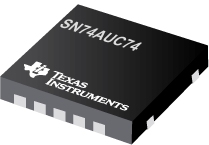

SN74AUC74是TI公司的一款D类触发器产品,SN74AUC74是具有清零和预设功能的双路上升沿 D 类触发器,本页介绍了SN74AUC74的产品说明、应用、特性等,并给出了与SN74AUC74相关的TI元器件型号供参考。
SN74AUC74 - 具有清零和预设功能的双路上升沿 D 类触发器 - D类触发器 - 触发器/锁存器/寄存器 - TI公司(Texas Instruments,德州仪器)
- Optimized for 1.8-V Operation and Is 3.6-V I/O Tolerant to Support Mixed-Mode Signal Operation
- Ioff Supports Partial-Power-Down Mode Operation
- Sub-1-V Operable
- Max tpd of 1.8 ns at 1.8 V
- Low Power Consumption, 10-µ Max ICC
- ±8-mA Output Drive at 1.8 V
- Latch-Up Performance Exceeds 100 mA Per JESD 78, Class II
- ESD Protection Exceeds JESD 22
- 2000-V Human-Body Model (A114-A)
- 200-V Machine Model (A115-A)
- 1000-V Charged-Device Model (C101)
DESCRIPTION/ORDERING INFORMATION
This dual positive-edge-triggered D-type flip-flop is operational at 0.8-V to 2.7-V VCC, but is designed specifically for 1.65-V to 1.95-V VCC operation.
A low level at the preset (PRE) or clear (CLR) inputs sets or resets the outputs, regardless of the levels of the other inputs. When PRE and CLR are inactive (high), data at the data (D) input meeting the setup time requirements is transferred to the outputs on the positive-going edge of the clock pulse. Clock triggering occurs at a voltage level and is not directly related to the rise time of the clock pulse. Following the hold-time interval, data at the D input can be changed without affecting the levels at the outputs. To better optimize the flip-flop for higher frequencies, the CLR input overrides the PRE input when they are both low.
This device is fully specified for partial-power-down applications using Ioff. The Ioff circuitry disables the outputs, preventing damaging current backflow through the device when it is powered down.


