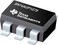

SN74AUP1G79是TI公司的一款无产品,SN74AUP1G79是低功耗单路上升沿 D 类触发器,本页介绍了SN74AUP1G79的产品说明、应用、特性等,并给出了与SN74AUP1G79相关的TI元器件型号供参考。
SN74AUP1G79 - 低功耗单路上升沿 D 类触发器 - 无 - 小尺寸逻辑器件 - TI公司(Texas Instruments,德州仪器)
- Available in the Texas Instruments NanoStar™ Package
- Low Static-Power Consumption: ICC = 0.9 µA Max
- Low Dynamic-Power Consumption: Cpd = 3 pF Typ at 3.3 V
- Low Input Capacitance: Ci = 1.5 pF Typ
- Low Noise: Overshoot and Undershoot < 10% of VCC
- Ioff Supports Partial Power-Down-Mode Operation
- Input Hysteresis Allows Slow Input Transition and Better Switching Noise Immunity at the Input (Vhys = 250 mV Typ at 3.3 V)
- Wide Operating VCC Range of 0.8 V to 3.6 V
- Optimized for 3.3-V Operation
- 3.6-V I/O Tolerant to Support Mixed-Mode Signal Operation
- tpd = 4 ns Max at 3.3 V
- Suitable for Point-to-Point Applications
- Latch-Up Performance Exceeds 100 mA Per JESD 78, Class II
- ESD Performance Tested Per JESD 22
- 2000-V Human-Body Model (A114-B, Class II)
- 1000-V Charged-Device Model (C101)
- Barcode Scanner
- Cable Solutions
- E-Book
- Embedded PC
- Field Transmitter: Temperature or Pressure Sensor
- Fingerprint Biometrics
- HVAC: Heating, Ventilating, and Air Conditioning
- Network-Attached Storage (NAS)
- Server Motherboard and PSU
- Software Defined Radio (SDR)
- TV: High-Definition (HDTV), LCD, and Digital
- Video Communications System
- Wireless Data Access Card, Headset, Keyboard, Mouse, and LAN Card
The AUP family is TI's premier solution to the industry's low-power needs in battery-powered portable applications. This family ensures a very low static and dynamic power consumption across the entire VCC range of 0.8 V to 3.6 V, thus resulting in an increased battery life. The AUP devices also maintain excellent signal integrity.
The SN74AUP1G79 is a single positive-edge-triggered D-type flip-flop. When data at the data (D) input meets the setup-time requirement, the data is transferred to the Q output on the positive-going edge of the clock pulse. Clock triggering occurs at a voltage level and is not directly related to the rise time of the clock pulse. Following the hold-time interval, data at the D input can be changed without affecting the levels at the outputs.
NanoStar™ package technology is a major breakthrough in IC packaging concepts, using the die as the package.
The SN74AUP1G79 device is fully specified for partial-power-down applications using Ioff. The Ioff circuitry disables the outputs, preventing damaging current backflow through the device when it is powered down.
| PART NUMBER | PACKAGE | BODY SIZE (NOM) |
|---|---|---|
| SN74AUP1G79 | SOT-23 (5) | 2.90 mm × 1.60 mm |
| SC70 (5) | 2.00 mm × 1.25 mm | |
| SOT (5) | 1.60 mm × 1.20 mm | |
| SON (6) | 1.45 mm × 1.00 mm | |
| SON (6) | 1.00 mm × 1.00 mm | |
| DSBGA (6) | 1.16 mm × 0.76 mm | |
| DSBGA (5) | 1.39 mm × 0.89 mm |


