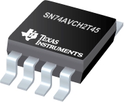

SN74AVCH2T45是TI公司的一款无产品,SN74AVCH2T45是具有可配置电压转换和 3 态输出的双位双电源总线收发器,本页介绍了SN74AVCH2T45的产品说明、应用、特性等,并给出了与SN74AVCH2T45相关的TI元器件型号供参考。
SN74AVCH2T45 - 具有可配置电压转换和 3 态输出的双位双电源总线收发器 - 无 - 小尺寸逻辑器件 - TI公司(Texas Instruments,德州仪器)
- Available in the Texas Instruments NanoFree™ Package
- VCC Isolation
- 2-Rail Design
- I/Os are 4.6 V Tolerant
- Partial Power-Down-Mode Operation
- Bus Hold on Data Inputs
- Maximum Data Rates
- 500 Mbps (1.8 V to 3.3 V)
- 320 Mbps (< 1.8 V to 3.3 V)
- 320 Mbps (Level-Shifting to 2.5 V or 1.8 V)
- 280 Mbps (Level-Shifting to 1.5 V)
- 240 Mbps (Level-Shifting to 1.2 V)
- Latch-Up Performance Exceeds 100 mA Per JESD 78, Class II
- ESD Protection Exceeds JESD 22
- Smartphone
- Servers
- Desktop PCs and Notebooks
- Other Portable Devices
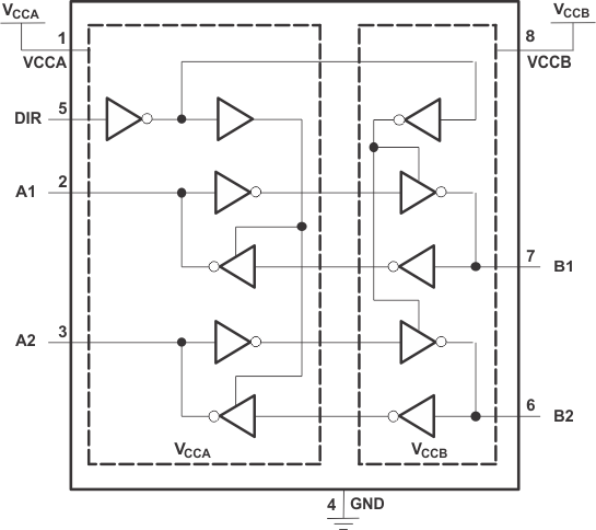
This 2-bit non-inverting bus transceiver uses two separate configurable power-supply rails. The A ports are designed to track VCCA and accepts any supply voltage from 1.2 V to 3.6 V. The B ports are designed to track VCCB and accepts any supply voltage from 1.2 V to 3.6 V. This allows for universal low-voltage bidirectional translation and level-shifting between any of the 1.2 V, 1.5 V, 1.8 V, 2.5 V, and 3.3 V voltage nodes.
The SN74AVCH2T45 is designed for asynchronous communication between two data buses. The logic levels of the direction-control (DIR pin) input activate either the B-port outputs or the A-port outputs. The device transmits data from the A bus to the B bus when the B-port outputs are activated and from the B bus to the A bus when the A-port outputs are activated. The SN74AVCH2T45 features active bus-hold circuitry, which holds unused or un-driven inputs at a valid logic state. TI does not recommend using pull-up or pull-down resistors with the bus-hold circuitry.
| PART NUMBER | PACKAGE | BODY SIZE (NOM) |
|---|---|---|
| SN74AVCH2T45 | SSOP (8) | 2.95 mm × 2.80 mm |
| VSSOP (8) | 2.30 mm × 2.00 mm | |
| DSBGA (8) | 1.89 mm × 0.89 mm |


