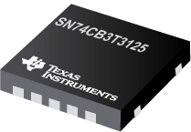

SN74CB3T3125是TI公司的一款数字开关产品,SN74CB3T3125是具有 5V 容限电平转换器的 3.3V 低电压四路 FET 总线开关,本页介绍了SN74CB3T3125的产品说明、应用、特性等,并给出了与SN74CB3T3125相关的TI元器件型号供参考。
SN74CB3T3125 - 具有 5V 容限电平转换器的 3.3V 低电压四路 FET 总线开关 - 数字开关 - 信号开关 - TI公司(Texas Instruments,德州仪器)
The SN74CB3T3125 is a high-speed TTL-compatible FET bus switch with low ON-state resistance (ron), allowing for minimal propagation delay. The device fully supports mixed-mode signal operation on all data I/O ports by providing voltage translation that tracks VCC. The SN74CB3T3125 supports systems using 5-V TTL, 3.3-V LVTTL, and 2.5-V CMOS switching standards, as well as user-defined switching levels (see ).
The SN74CB3T3125 is organized as four 1-bit bus switches with separate output-enable (1OE, 2OE, 3OE, 4OE) inputs. It can be used as four 1-bit bus switches or as one 4-bit bus switch. When OE is low, the associated 1-bit bus switch is ON, and the A port is connected to the B port, allowing bidirectional data flow between ports. When OE is high, the associated 1-bit bus switch is OFF, and the high-impedance state exists between the A and B ports.
This device is fully specified for partial-power-down applications using Ioff. The Ioff feature ensures that damaging current will not backflow through the device when it is powered down. The device has isolation during power off.
To ensure the high-impedance state during power up or power down, OE should be tied to VCC through a pullup resistor; the minimum value of the resistor is determined by the current-sinking capability of the driver.
- Output Voltage Translation Tracks VCC
- Supports Mixed-Mode Signal Operation On All Data I/O Ports
- 5-V Input Down to 3.3-V Output-Level Shift With 3.3-V VCC
- 5-V/3.3-V Input Down to 2.5-V Output-Level Shift With 2.5-V VCC
- 5-V-Tolerant I/Os With Device Powered Up or Powered Down
- Bidirectional Data Flow, With Near-Zero Propagation Delay
- Low ON-State Resistance (ron) Characteristics ron = 5 Ω Typ)
- Low Input/Output Capacitance Minimizes Loading (Cio(OFF) = 4.5 pF Typ)
- Data and Control Inputs Provide Undershoot Clamp Diodes
- Low Power Consumption (ICC = 20 µA Max)
- VCC Operating Range From 2.3 V to 3.6 V
- Data I/Os Support 0- to 5-V Signaling Levels (0.8 V, 1.2 V, 1.5 V, 1.8 V, 2.5 V, 3.3 V, 5 V)
- Control Inputs Can Be Driven by TTL or 5-V/3.3-V CMOS Outputs
- Ioff Supports Partial-Power-Down Mode Operation
- Latch-Up Performance Exceeds 250 mA Per JESD 17
- ESD Performance Tested Per JESD 22
- 2000-V Human-Body Model (A114-B, Class II)
- 1000-V Charged-Device Model (C101)
- Supports Digital Applications: Level Translation, USB Interface, Bus Isolation
- Ideal for Low-Power Portable Equipment


