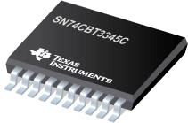

SN74CBT3345C是TI公司的一款数字开关产品,SN74CBT3345C是具有 -2V 下冲保护的 8 位 FET 总线开关,本页介绍了SN74CBT3345C的产品说明、应用、特性等,并给出了与SN74CBT3345C相关的TI元器件型号供参考。
SN74CBT3345C - 具有 -2V 下冲保护的 8 位 FET 总线开关 - 数字开关 - 信号开关 - TI公司(Texas Instruments,德州仪器)
The SN74CBT3345C is a high-speed TTL-compatible FET bus switch with low ON-state resistance (ron), allowing for minimal propagation delay. Active Undershoot-Protection Circuitry on the A and B ports of the SN74CBT3345C provides protection for undershoot up to –2 V by sensing an undershoot event and ensuring that the switch remains in the proper OFF state.
The SN74CBT3345C is organized as an 8-bit bus switch with two output-enable (OE, OE\) inputs. When OE is high or OE\ is low, the bus switch is ON, and the A port is connected to the B port, allowing bidirectional data flow between ports. When OE is low and OE\ is high, the bus switch is OFF and the high-impedance state exists between the A and B ports.
This device is fully specified for partial-power-down applications using Ioff. The Ioff feature ensures that damaging current will not backflow through the device when it is powered down.
To ensure the high-impedance state during power up or power down, OE\ should be tied to VCC through a pullup resistor and OE should be tied to GND through a pulldown resistor; the minimum value of the resistor is determined by the current-sinking/current-sourcing capability of the driver.
- Undershoot Protection for Off-Isolation on A and B Ports Up to –2 V
- Bidirectional Data Flow, With Near-Zero Propagation Delay
- Low ON-State Resistance (ron) Characteristics (ron = 3 Typical)
- Low Input/Output Capacitance Minimizes Loading and Signal Distortion Cio(OFF) = 5.5 pF Typical)
- Data and Control Inputs Provide Undershoot Clamp Diodes
- Low Power Consumption ICC = 3 µA Max)
- VCC Operating Range From 4 V to 5.5 V
- Data I/Os Support 0 to 5-V Signaling Levels (0.8-V, 1.2-V, 1.5-V, 1.8-V, 2.5-V, 3.3-V, 5-V)
- Control Inputs Can Be Driven by TTL or 5-V/3.3-V CMOS Outputs
- Ioff Supports Partial-Power-Down Mode Operation
- Latch-Up Performance Exceeds 100 mA Per JESD 78, Class II
- ESD Performance Tested Per JESD 22
- 2000-V Human-Body Model (A114-B, Class II)
- 1000-V Charged-Device Model (C101)
- Supports Both Digital and Analog Applications: USB Interface, Memory Interleaving, Bus Isolation, Low-Distortion Signal Gating


