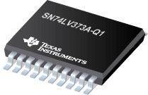

SN74LV373A-Q1是TI公司的一款D类锁存器产品,SN74LV373A-Q1是汽车类具有三态输出的八路透明 D 类锁存器,本页介绍了SN74LV373A-Q1的产品说明、应用、特性等,并给出了与SN74LV373A-Q1相关的TI元器件型号供参考。
SN74LV373A-Q1 - 汽车类具有三态输出的八路透明 D 类锁存器 - D类锁存器 - 触发器/锁存器/寄存器 - TI公司(Texas Instruments,德州仪器)
- Qualified for Automotive Applications
- 2-V to 5.5-V VCC Operation
- Maximum tpd of 8.5 ns at 5 V
- Typical VOLP (Output Ground Bounce) < 0.8 V at VCC = 3.3 V, TA = 25°C
- Typical VOHV (Output VOH Undershoot)> 2.3 V at VCC = 3.3 V, TA = 25°C
- Supports Mixed-Mode Voltage Operation on All Ports
- Ioff Supports Partial-Power-Down Mode Operation
- Latch-Up Performance Exceeds 250 mA Per JESD 17
DESCRIPTION/ORDERING INFORMATION
The SN74LV373A device is an octal transparent D-type latch designed for 2-V to 5.5-V VCC operation.
While the latch-enable (LE) input is high, the Q outputs follow the data (D) inputs. When LE is taken low, the Q outputs are latched at the logic levels set up at the D inputs.
A buffered output-enable (OE) input can be used to place the eight outputs in either a normal logic state (high or low) or the high-impedance state. In the high-impedance state, the outputs neither load nor drive the bus lines significantly. The high-impedance state and increased drive provide the capability to drive bus lines without need for interface or pullup components.
OE does not affect the internal operations of the latches. Old data can be retained or new data can be entered while the outputs are in the high-impedance state.
To ensure the high-impedance state during power up or power down, OE shall be tied to VCC through a pullup resistor; the minimum value of the resistor is determined by the current-sinking capability of the driver.
This device is fully specified for partial-power-down applications using Ioff. The Ioff circuitry disables the outputs, preventing damaging current backflow through the device when it is powered down.


