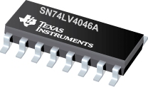

SN74LV4046A是TI公司的一款锁相环(PLL)/振荡器产品,SN74LV4046A是特殊逻辑,本页介绍了SN74LV4046A的产品说明、应用、特性等,并给出了与SN74LV4046A相关的TI元器件型号供参考。
SN74LV4046A - 特殊逻辑 - 锁相环(PLL)/振荡器 - 特殊逻辑 - TI公司(Texas Instruments,德州仪器)
- Choice of Three Phase Comparators
- Exclusive OR
- Edge-Triggered J-K Flip-Flop
- Edge-Triggered RS Flip-Flop
- Excellent VCO Frequency Linearity
- VCO-Inhibit Control for ON/OFF Keying and for Low Standby Power Consumption
- Optimized Power-Supply Voltage Range From 3 V to 5.5 V
- Wide Operating Temperature Range . . . –40°C to 125°C
- Latch-Up Performance Exceeds 250 mA Per JESD 17
- ESD Protection Exceeds JESD 22
- 2000-V Human Body Model (A114-A)
- 200-V Machine Model (A115-A)
- 1000-V Charged-Device Model (C101)
- Telecommunications
- Signal Generators
- Digital Phase-Locked Loop
The SN74LV4046A is a high-speed silicon-gate CMOS device that is pin compatible with the CD4046B and the CD74HC4046. The device is specified in compliance with JEDEC Std 7.
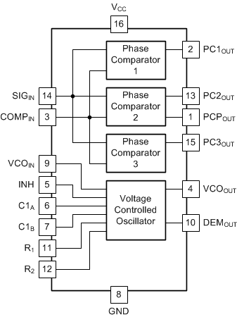
The SN74LV4046A is a phase-locked loop (PLL) circuit that contains a linear voltage-controlled oscillator (VCO) and three different phase comparators (PC1, PC2, and PC3). A signal input and a comparator input are common to each comparator.
The signal input can be directly coupled to large voltage signals, or indirectly coupled (with a series capacitor) to small voltage signals. A self-bias input circuit keeps small voltage signals within the linear region of the input amplifiers. With a passive low-pass filter, the SN74LV4046A forms a second-order loop PLL. The excellent VCO linearity is achieved by the use of linear operational amplifier techniques. Various applications include telecommunications, digital phase-locked loop and signal generators.
| PART NUMBER | PACKAGE | BODY SIZE (NOM) |
|---|---|---|
| SN74LV4046A | SOP (16) | 7.70mm x 10.20mm |
| SOIC (16) | 6.00mm x 9.90mm | |
| TSSOP (16) | 6.40mm x 5.00mm |


