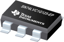

SN74LVC1G125-EP是TI公司的一款无产品,SN74LVC1G125-EP是具有三态输出的增强型产品单路总线缓冲器闸,本页介绍了SN74LVC1G125-EP的产品说明、应用、特性等,并给出了与SN74LVC1G125-EP相关的TI元器件型号供参考。
SN74LVC1G125-EP - 具有三态输出的增强型产品单路总线缓冲器闸 - 无 - 小尺寸逻辑器件 - TI公司(Texas Instruments,德州仪器)
- Controlled Baseline
- One Assembly/Test Site, One Fabrication Site
- Enhanced Diminishing Manufacturing Sources (DMS) Support
- Enhanced Product-Change Notification
- Qualification Pedigree(1)Component qualification in accordance with JEDEC and industry standards to ensure reliable operation over an extended temperature range. This includes, but is not limited to, Highly Accelerated Stress Test (HAST) or biased 85/85, temperature cycle, autoclave or unbiased HAST, electromigration, bond intermetallic life, and mold compound life. Such qualification testing should not be viewed as justifying use of this component beyond specified performance and environmental limits.
- Supports 5-V VCC Operation
- Inputs Accept Voltages to 5.5 V
- Max tpd of 3.7 ns at 3.3 V
- Low Power Consumption, 10-µA Max ICC
- ±24-mA Output Drive at 3.3 V
- Ioff Supports Partial-Power-Down Mode Operation
- Latch-Up Performance Exceeds 100 mA Per JESD 78, Class II
- ESD Protection Exceeds JESD 22
- 2000-V Human-Body Model (A114-A)
- 200-V Machine Model (A115-A)
- 1000-V Charged-Device Model (C101)
(1)Component qualification in accordance with JEDEC and industry standards to ensure reliable operation over an extended temperature range. This includes, but is not limited to, Highly Accelerated Stress Test (HAST) or biased 85/85, temperature cycle, autoclave or unbiased HAST, electromigration, bond intermetallic life, and mold compound life. Such qualification testing should not be viewed as justifying use of this component beyond specified performance and environmental limits.
DESCRIPTION/ORDERING INFORMATION
This bus buffer gate is designed for 1.65-V to 5.5-V VCC operation.
The SN74LVC1G125 is a single line driver with a 3-state output. The output is disabled when the output-enable (OE) input is high.
This device is fully specified for partial-power-down applications using Ioff. The Ioff circuitry disables the outputs, preventing damaging current backflow through the device when it is powered down.
To ensure the high-impedance state during power up or power down, OE should be tied to VCC through a pullup resistor; the minimum value of the resistor is determined by the current-sinking capability of the driver.


