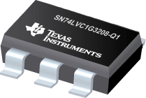

SN74LVC1G3208-Q1是TI公司的一款无产品,SN74LVC1G3208-Q1是汽车类单路 3 输入正或与门,本页介绍了SN74LVC1G3208-Q1的产品说明、应用、特性等,并给出了与SN74LVC1G3208-Q1相关的TI元器件型号供参考。
SN74LVC1G3208-Q1 - 汽车类单路 3 输入正或与门 - 无 - 小尺寸逻辑器件 - TI公司(Texas Instruments,德州仪器)
This device is designed for 1.65-V to 5.5-V VCC operation.
The SN74LVC1G3208-Q1 is a single 3-input positive OR-AND gate. It performs the Boolean function Y = (A + B) ⋅ C in positive logic.
By tying one input to GND or VCC, the SN74LVC1G3208-Q1 offers two more functions. When C is tied to VCC, this device performs as a 2-input OR gate (Y = A + B). When A is tied to GND, the device works as a 2-input AND gate (Y = B ⋅ C). This device also works as a 2-input AND gate when B is tied to GND (Y = A ⋅ C).
This device is fully specified for partial-power-down applications using Ioff. The Ioff circuitry disables the outputs, preventing damaging current backflow through the device when it is powered down.
- Qualified for Automotive Applications
- Supports 5-V VCC Operation
- Inputs Accept Voltages to 5.5 V
- Max tpd of 5 ns at 3.3 V
- Low Power Consumption, 10-μA Max ICC
- ±24-mA Output Drive at 3.3 V
- Input Hysteresis Allows Slow Input Transition and Better Switching Noise Immunity at the Input(Vhys = 250 mV Typ at 3.3 V)
- Can Be Used in Three Combinations:
- OR-AND Gate
- OR Gate
- AND Gate
- Ioff Supports Partial-Power-Down Mode Operation


