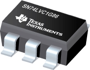

SN74LVC1G86是TI公司的一款TI芯片产品,SN74LVC1G86是单路 2 输入异或门,本页介绍了SN74LVC1G86的产品说明、应用、特性等,并给出了与SN74LVC1G86相关的TI元器件型号供参考。
SN74LVC1G86 - 单路 2 输入异或门 - TI芯片 - 小尺寸逻辑器件 - TI公司(Texas Instruments,德州仪器)
- Available in the Texas Instruments NanoFree™ Package
- Supports 5-V VCC Operation
- Inputs Accept Voltages to 5.5 V
- Supports Down Translation to VCC
- Maximum tpd of 4 ns at 3.3 V and 15-pF load
- Low Power Consumption, 10-µA Maximum ICC
- ±24-mA Output Drive at 3.3 V
- Ioff Supports Live Insertion, Partial-Power-Down Mode, and Back-Drive Protection
- Latch-Up Performance Exceeds 100 mA Per JESD 78, Class II
- ESD Protection Exceeds JESD 22
- 2000-V Human-Body Model (A114-A)
- 1000-V Charged-Device Model (C101)
- Cameras
- Programmable Logic Controllers
- Telecom Infrastructure
- Wireless Headsets
- Motor Drives and Controls
- TVs
- Set-Top Boxes
- Audio
The SN74LVC1G86 device performs the Boolean function Y = A × B or Y = AB + AB in positive logic. This single 2-input exclusive-OR gate is designed for 1.65-V to 5.5-V VCC operation.
If the input is low, the other input is reproduced in true form at the output. If the input is high, the signal on the other input is reproduced inverted at the output. This device has low power consumption with maximum tpd of 4 ns at 3.3 V and 15-pF capacitive load. The max output drive is ±32-mA at 4.5 V and ±24-mA at 3.3 V.
This device is fully specified for partial-power-down applications using Ioff. The Ioff circuitry disables the outputs, preventing damaging current back flow through the device when it is powered down.
| PART NUMBER | PACKAGE | BODY SIZE (NOM) |
|---|---|---|
| SN74LVC1G86DBV | SOT-23 (5) | 2.90 mm × 1.60 mm |
| SN74LVC1G86DCK | SC70 (5) | 2.00 mm × 1.25 mm |
| SN74LVC1G86DRL | SOT (5) | 1.60 mm × 1.20 mm |
| SN74LVC1G86YZP | DSBGA (5) | 1.44 mm × 0.94 mm |


