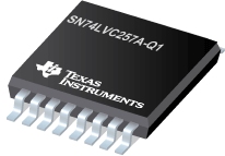

SN74LVC257A-Q1是TI公司的一款解码器/编码器/多路复用器产品,SN74LVC257A-Q1是汽车类具有三态输出的四路 2 线路至 1 线路数据选择器/多路复用器,本页介绍了SN74LVC257A-Q1的产品说明、应用、特性等,并给出了与SN74LVC257A-Q1相关的TI元器件型号供参考。
SN74LVC257A-Q1 - 汽车类具有三态输出的四路 2 线路至 1 线路数据选择器/多路复用器 - 解码器/编码器/多路复用器 - 特殊逻辑 - TI公司(Texas Instruments,德州仪器)
The SN74LVC257A quadruple 2-line to 1-line data selector/multiplexer is designed for 2.7-V to 3.6-V VCC operation.
The device is designed for high-performance memory-decoding or data-routing applications requiring very short propagation delay times. In high-performance memory systems, this decoder minimizes the effects of system decoding. When employed with high-speed memories utilizing a fast enable circuit, delay times of this decoder and the enable time of the memory usually are less than the typical access time of the memory. This means that the effective system delay introduced by the decoder is negligible.
The conditions at the binary-select inputs and the three enable inputs select one of eight output lines. Two active-low enable inputs and one active-high enable input reduce the need for external gates or inverters when expanding. A 24-line decoder can be implemented without external inverters, and a 32-line decoder requires only one inverter. An enable input can be used as a data input for demultiplexing applications.
Inputs can be driven from either 3.3-V or 5-V devices. This feature allows the use of this device as a translator in a mixed 3.3-V/5-V system environment.
- Qualified for Automotive Applications
- ESD Protection Exceeds 2000 V Per MIL-STD-883, Method 3015; Exceeds 200 V Using Machine Model (C = 200 pF, R = 0)
- Operates From 2 V to 3.6 V
- Inputs Accept Voltages to 5.5 V
- Max tpd of 4.6 ns at 3.3 V
- Typical VOLP (Output Ground Bounce) <0.8 V at VCC = 3.3 V, TA = 25°C
- Typical VOHV (Output VOH Undershoot) >2 V at VCC = 3.3 V, TA = 25°C


