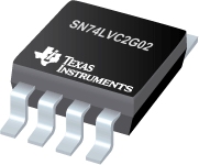

SN74LVC2G02 - 双路 2 输入正或非门
SN74LVC2G02是TI公司的一款无产品,SN74LVC2G02是双路 2 输入正或非门,本页介绍了SN74LVC2G02的产品说明、应用、特性等,并给出了与SN74LVC2G02相关的TI元器件型号供参考。
SN74LVC2G02 - 双路 2 输入正或非门 - 无 - 小尺寸逻辑器件 - TI公司(Texas Instruments,德州仪器)
产品描述
This dual 2-input positive-NOR gate is designed for 1.65-V to 5.5-V VCC operation.
The SN74LVC2G02 performs the Boolean function Y = A + B or Y = A•B in positive logic.
NanoFree™ package technology is a major breakthrough in IC packaging concepts, using the die as the package.
This device is fully specified for partial-power-down applications using Ioff. The Ioff circuitry disables the outputs, preventing damaging current backflow through the device when it is powered down.
产品特性
- Available in the Texas Instruments NanoFree Package
- Supports 5-V VCC Operation
- Inputs Accept Voltages to 5.5 V
- Max tpd of 4.9 ns at 3.3 V
- Low Power Consumption, 10-μA Max ICC
- ±24-mA Output Drive at 3.3 V
- Typical VOLP (Output Ground Bounce) <0.8 V at VCC = 3.3 V, TA = 25°C
- Typical VOHV (Output VOH Undershoot) >2 V at VCC = 3.3 V, TA = 25°C
- Ioff Supports Partial-Power-Down Mode Operation
- Latch-Up Performance Exceeds 100 mA Per JESD 78, Class II
- ESD Protection Exceeds JESD 22
- 2000-V Human-Body Model (A114-A)
- 1000-V Charged-Device Model (C101)
下面可能是您感兴趣的TI公司无元器件


TI公司产品现货专家,订购TI公司产品不限最低起订量,TI产品大陆现货即时发货,香港库存3-5天发货,海外库存7-10天发货
寻找全球TI代理商现货货源 - TI公司(德州仪器)电子元件在线订购


