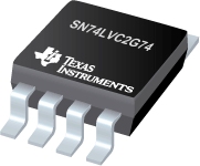

SN74LVC2G74是TI公司的一款TI芯片产品,SN74LVC2G74是具有清零和预设功能的单路上升沿 D 类触发器,本页介绍了SN74LVC2G74的产品说明、应用、特性等,并给出了与SN74LVC2G74相关的TI元器件型号供参考。
SN74LVC2G74 - 具有清零和预设功能的单路上升沿 D 类触发器 - TI芯片 - 小尺寸逻辑器件 - TI公司(Texas Instruments,德州仪器)
- Available in the Texas Instruments NanoFree™ Package
- Supports 5-V VCC Operation
- Inputs Accept Voltages to 5.5 V
- Max tpd of 5.9 ns at 3.3 V
- Low Power Consumption, 10-μA Max ICC
- ±24-mA Output Drive at 3.3 V
- Typical VOLP (Output Ground Bounce) < 0.8 V at VCC = 3.3 V, TA = 25°C
- Typical VOHV (Output VOH Undershoot) > 2 V at VCC = 3.3 V, TA = 25°C
- Ioff Supports Live Insertion, Partial-Power-Down Mode, and Back-Drive Protection
- Latch-Up Performance Exceeds 100 mA Per JESD 78, Class II
- ESD Protection Exceeds JESD 22
- 2000-V Human-Body Model
- 200-V Machine Model
- 1000-V Charged-Device Model
- Servers
- LED displays
- Network switch
- Telecom infrastructure
- Motor drivers
- I/O Expanders
This single positive-edge-triggered D-type flip-flop is designed for 1.65-V to 5.5-V VCC operation.
NanoFree™ package technology is a major breakthrough in IC packaging concepts, using the die as the package.
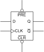
A low level at the preset (PRE) or clear (CLR) input sets or resets the outputs, regardless of the levels of the other inputs. When PRE and CLR are inactive (high), data at the data (D) input meeting the setup time requirements is transferred to the outputs on the positive-going edge of the clock pulse. Clock triggering occurs at a voltage level and is not related directly to the rise time of the clock pulse. Following the hold-time interval, data at the D input can be changed without affecting the levels at the outputs.
This device is fully specified for partial-power-down applications using Ioff. The Ioff circuitry disables the outputs, preventing damaging current backflow through the device when it is powered down.
| PART NUMBER | PACKAGE | BODY SIZE |
|---|---|---|
| SN74LVC2G74 | SSOP (8) | 2.95 mm × 2.80 mm |
| VSSOP (8) | 2.30 mm × 2.00 mm | |
| DSBGA (8) | 1.91 mm × 0.91 mm |


