
SN74LVC2T45是TI公司的一款无产品,SN74LVC2T45是具有可配置电压转换和三态输出的 2 位双电源总线收发器,本页介绍了SN74LVC2T45的产品说明、应用、特性等,并给出了与SN74LVC2T45相关的TI元器件型号供参考。
SN74LVC2T45 - 具有可配置电压转换和三态输出的 2 位双电源总线收发器 - 无 - 小尺寸逻辑器件 - TI公司(Texas Instruments,德州仪器)
- Available in the Texas Instruments NanoFree™ Package
- Fully Configurable Dual-Rail Design Allows Each Port to Operate Over the Full 1.65-V to 5.5-V Power-Supply Range
- VCC Isolation Feature – If Either VCC Input Is at GND, Both Ports Are in the High-Impedance State
- DIR Input Circuit Referenced to VCCA
- Low Power Consumption, 10-μA Max ICC
- ±24-mA Output Drive at 3.3 V
- Ioff Supports Partial-Power-Down Mode Operation
- Max Data Rates
- 420 Mbps (3.3-V to 5-V Translation)
- 210 Mbps (Translate to 3.3 V)
- 140 Mbps (Translate to 2.5 V)
- 75 Mbps (Translate to 1.8 V)
- Latch-Up Performance Exceeds 100 mA Per JESD 78, Class II
- ESD Protection Exceeds JESD 22
- 4000-V Human-Body Model (A114-A)
- 200-V Machine Model (A115-A)
- 1000-V Charged-Device Model (C101)
- Personal Electronic
- Industrial
- Enterprise
- Telecom
This dual-bit noninverting bus transceiver uses two separate configurable power-supply rails. The A port is designed to track VCCA. VCCA accepts any supply voltage from 1.65 V to 5.5 V. The B port is designed to track VCCB. VCCB accepts any supply voltage from 1.65 V to 5.5 V. This allows for universal low-voltage bidirectional translation between any of the 1.8-V, 2.5-V, 3.3-V, and 5-V voltage nodes.
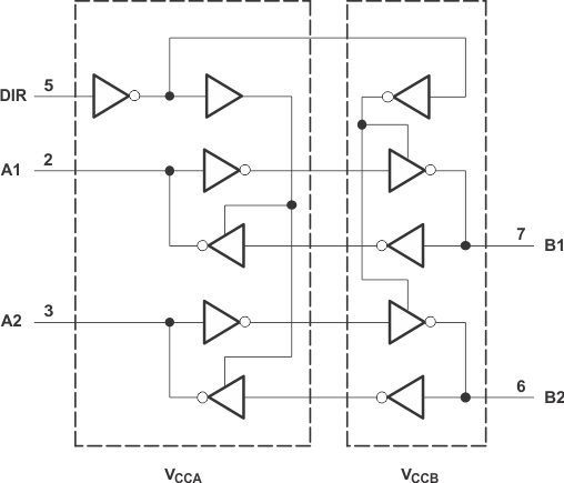
The SN74LVC2T45 is designed for asynchronous communication between two data buses. The logic levels of the direction-control (DIR) input activate either the B-port outputs or the A-port outputs. The device transmits data from the A bus to the B bus when the B-port outputs are activated, and from the B bus to the A bus when the A-port outputs are activated. The input circuitry on both A and B ports always is active and must have a logic HIGH or LOW level applied to prevent excess ICC and ICCZ.
The SN74LVC2T45 is designed so that the DIR input circuit is supplied by VCCA. This device is fully specified for partial-power-down applications using Ioff. The Ioff circuitry disables the outputs, preventing damaging current backflow through the device when it is powered down.
The VCC isolation feature ensures that if either VCC input is at GND, both ports are in the high-impedance state. NanoFree™ package technology is a major breakthrough in IC packaging concepts, using the die as the package.
| PART NUMBER | PACKAGE | BODY SIZE (NOM) |
|---|---|---|
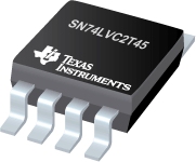
| SN74LVC2T45 | SSOP (8) | 2.95 mm x 2.80 mm |
| VSSOP (8) | 2.30 mm x 2.00 mm | |
| DSBGA (8) | 1.89 mm x 0.89 mm |


