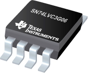

SN74LVC3G06是TI公司的一款无产品,SN74LVC3G06是具有漏极开路输出的三路反向器缓冲器/驱动器,本页介绍了SN74LVC3G06的产品说明、应用、特性等,并给出了与SN74LVC3G06相关的TI元器件型号供参考。
SN74LVC3G06 - 具有漏极开路输出的三路反向器缓冲器/驱动器 - 无 - 小尺寸逻辑器件 - TI公司(Texas Instruments,德州仪器)
This triple inverter buffer/driver is designed for 1.65-V to 5.5-V VCC operation.
The output of the SN74LVC3G06 is open drain and can be connected to other open-drain outputs to implement active-low wired-OR or active-high wired-AND functions. The maximum sink current is 32 mA.
NanoFree™ package technology is a major breakthrough in IC packaging concepts, using the die as the package.
This device is fully specified for partial-power-down applications using Ioff. The Ioff circuitry disables the outputs, preventing damaging current backflow through the device when it is powered down.
- Available in the Texas Instruments NanoFree Package
- Supports 5-V VCC Operation
- Input and Open-Drain Output Accepts Voltages up to 5.5 V
- Max tpd of 3.4 ns at 3.3 V
- Low Power Consumption, 10-μA Max ICC
- ±24-mA Output Drive at 3.3 V
- Typical VOLP (Output Ground Bounce) < 0.8 V at VCC = 3.3 V, TA = 25°C
- Typical VOHV (Output VOH Undershoot) > 2 V at VCC = 3.3 V, TA = 25°C
- Ioff Supports Live Insertion, Partial-Power-Down Mode and Back Drive Protection
- Latch-Up Performance Exceeds 100 mA Per JESD 78, Class II
- ESD Protection Exceeds JESD 22
- 2000-V Human-Body Model (A114-A)
- 200-V Machine Model (A115-A)
- 1000-V Charged-Device Model (C101)


