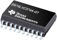

SN74LVC574A-Q1是TI公司的一款D类触发器产品,SN74LVC574A-Q1是汽车类具有三态输出的八路边沿 D 类触发器,本页介绍了SN74LVC574A-Q1的产品说明、应用、特性等,并给出了与SN74LVC574A-Q1相关的TI元器件型号供参考。
SN74LVC574A-Q1 - 汽车类具有三态输出的八路边沿 D 类触发器 - D类触发器 - 触发器/锁存器/寄存器 - TI公司(Texas Instruments,德州仪器)
- Qualified for Automotive Applications
- ESD Protection Exceeds 2000 V Per MIL-STD-883, Method 3015; Exceeds 200 V Using Machine Model (C = 200 pF, R = 0)
- Operates From 2 V to 3.6 V
- Inputs Accept Voltages to 5.5 V
- Max tpd of 7 ns at 3.3 V
- Typical VOLP (Output Ground Bounce) < 0.8 V at VCC = 3.3 V, TA = 25°C
- Typical VOHV (Output VOH Undershoot) > 2 V at VCC = 3.3 V, TA = 25°C
- Supports Mixed-Mode Signal Operation on All Ports (5-V Input/Output Voltage With 3.3-V VCC)
- Ioff Supports Partial-Power-Down Mode Operation
DESCRIPTION/ORDERING INFORMATION
The SN74LVC574A octal edge-triggered D-type flip-flop is designed for 2.7-V to 3.6-V VCC operation.
This device features 3-state outputs designed specifically for driving highly capacitive or relatively low-impedance loads. It is particularly suitable for implementing buffer registers, I/O ports, bidirectional bus drivers, and working registers.
On the positive transition of the clock (CLK) input, the Q outputs are set to the logic levels at the data (D) inputs.
A buffered output-enable (OE) input can be used to place the eight outputs in either a normal logic state (high or low logic levels) or the high-impedance state. In the high-impedance state, the outputs neither load nor drive the bus lines significantly. The high-impedance state and increased drive provide the capability to drive bus lines without interface or pullup components.
OE does not affect the internal operations of the flip-flops. Old data can be retained or new data can be entered while the outputs are in the high-impedance state.
This device is fully specified for partial-power-down applications using Ioff. The Ioff circuitry disables the outputs, preventing damaging current backflow through the device when it is powered down.
To ensure the high-impedance state during power up or power down, OE should be tied to VCC through a pullup resistor; the minimum value of the resistor is determined by the current-sinking capability of the driver.
Inputs can be driven from either 3.3-V or 5-V devices. This feature allows the use of thIs device as a translator in a mixed 3.3-V/5-V system environment.


