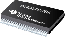

SN74LVCZ161284A是TI公司的一款IEEE-1284并行端接口(PPI)产品,SN74LVCZ161284A是19 位 IEEE 1284 标准总线接口,本页介绍了SN74LVCZ161284A的产品说明、应用、特性等,并给出了与SN74LVCZ161284A相关的TI元器件型号供参考。
SN74LVCZ161284A - 19 位 IEEE 1284 标准总线接口 - IEEE-1284并行端接口(PPI) - 特殊逻辑 - TI公司(Texas Instruments,德州仪器)
The SN74LVCZ161284A is designed for 3-V to 3.6-V VCC operation. This device provides asynchronous two-way communication between data buses. The control-function implementation minimizes external timing requirements.
This device has eight bidirectional bits; data can flow in the A-to-B direction when the direction-control input (DIR) is high, and in the B-to-A direction when DIR is low. This device also has five drivers that drive the cable side, and four receivers. The SN74LVCZ161284A has one receiver dedicated to the HOST LOGIC line and a driver to drive the PERI LOGIC line.
The output drive mode is determined by the high-drive (HD) control pin. When HD is high, the outputs are in a totem-pole configuration, and in an open-drain configuration when HD is low. This meets the drive requirements as specified in the IEEE Std 1284-I (level-1 type) and IEEE Std 1284-II (level-2 type) parallel peripheral-interface specifications. Except for HOST LOGIC IN and peripheral logic out (PERI LOGIC OUT), all cable-side pins have a 1.4-k integrated pullup resistor. The pullup resistor is switched off if the associated output driver is in the low state or if the output voltage is above VCC CABLE. If VCC CABLE is off, PERI LOGIC OUT is set to low.
The device has two supply voltages. VCC is designed for 3-V to 3.6-V operation. VCC CABLE supplies the inputs and output buffers of the cable side only and is designed for 3-V to 3.6-V and for 4.7-V to 5.5-V operation. Even when VCC CABLE is 3 V to 3.6 V, the cable-side I/O pins are 5-V tolerant.
The Power-On Reset (POR) ensures that the Y outputs (Y9–Y13) stay in the high state after power on until an associated input (A9–A13) goes high. When an associated input goes high, all Y outputs are activated, and noninverting signals of the associated inputs are driven through Y outputs. This special feature prevents printer system errors caused by deasserting the BUSY signal in the cable at power on.
- Power-On Reset (POR) Prevents Printer Errors When Printer Is Turned On, But No Valid Signal Is at Pins A9–A13
- Operates From 3 V to 3.6 V
- 1.4-k Pullup Resistors Integrated on All Open-Drain Outputs Eliminate the Need for Discrete Resistors
- Designed for the IEEE Std 1284-I (Level-1 Type) and IEEE Std 1284-II (Level-2 Type) Electrical Specifications
- Flow-Through Architecture Optimizes PCB Layout
- Ioff and Power-Up 3-State Support Hot Insertion
- Latch-Up Performance Exceeds 100 mA Per JESD 78, Class II
- ESD Protection Exceeds JESD 22
- 4000-V Human-Body Model (A114-A)
- 350-V Machine Model (A115-A)
- 1500-V Charged-Device Model (C101)


