


SN75176A是TI公司的一款无产品,SN75176A是差动总线收发器,本页介绍了SN75176A的产品说明、应用、特性等,并给出了与SN75176A相关的TI元器件型号供参考。
SN75176A - 差动总线收发器 - 无 - RS-485收发器 - TI公司(Texas Instruments,德州仪器)
- Bidirectional Transceiver
- Meets or Exceeds the Requirements of ANSI Standards EIA/TIA-422-B and ITU Recommendations V.11
- Designed for Multipoint Transmission on Long Bus Lines in Noisy Environments
- 3-State Driver and Receiver Outputs
- Individual Driver and Receiver Enables
- Wide Positive and Negative Input/Output Bus Voltage Ranges
- Driver Output Capability ±60 mA Max
- Thermal-Shutdown Protection
- Driver Positive-Current Limiting and Negative-Current Limiting
- Receiver Input Impedance 12 kΩ Min
- Receiver Input Sensitivity ±200 mV
- Receiver Input Hysteresis 50 mV Typ
- Operates From Single 5-V Supply
- Lower Power Requirements
- Low Speed RS485 communication (5 Mbps or less)
- For 10 Mbps, use SN75176B
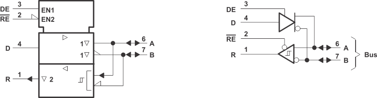
The SN75176A differential bus transceiver is a monolithic integrated circuit designed for bidirectional data communication on multipoint bus-transmission lines. It is designed for balanced transmission lines and meets ANSI Standard EIA/TIA-422-B and ITU Recommendation V.11.
The SN75176A combines a 3-state differential line driver and a differential input line receiver, both of which operate from a single 5-V power supply. The driver and receiver have active-high and active-low enables, respectively, that can be externally connected together to function as a direction control. The driver differential outputs and the receiver differential inputs are connected internally to form differential input/output (I/O) bus ports that are designed to offer minimum loading to the bus whenever the driver is disabled or VCC = 0. These ports feature wide positive and negative common-mode voltage ranges making the device suitable for party-line applications.
The driver is designed to handle loads up to 60 mA of sink or source current. The driver features positive- and negative-current limiting and thermal shutdown for protection from line fault conditions. Thermal shutdown is designed to occur at a junction temperature of approximately 150°C. The receiver features a minimum input impedance of 12 kΩ, an input sensitivity of ±200 mV, and a typical input hysteresis of 50 mV.
The SN75176A can be used in transmission-line applications employing the SN75172 and SN75174 quadruple differential line drivers and SN75173 and SN75175 quadruple differential line receivers.
The SN75176A is characterized for operation from 0°C to 70°C.
| PART NUMBER | PACKAGE (PIN) | BODY SIZE (NOM) |
|---|---|---|
| SN75176A | SOIC (8) | 4.90 mm × 3.91 mm |
| PDIP (8) | 9.81 mm × 6.35 mm |

