
SN75176B是TI公司的一款无产品,SN75176B是差动总线收发器,本页介绍了SN75176B的产品说明、应用、特性等,并给出了与SN75176B相关的TI元器件型号供参考。
SN75176B - 差动总线收发器 - 无 - RS-485收发器 - TI公司(Texas Instruments,德州仪器)
- Bidirectional Transceivers
- Meet or Exceed the Requirements of ANSI Standards TIA/EIA-422-B and TIA/EIA-485-A and ITU Recommendations V.11 and X.27
- Designed for Multipoint Transmission on Long Bus Lines in Noisy Environments
- 3-State Driver and Receiver Outputs
- Individual Driver and Receiver Enables
- Wide Positive and Negative Input/Output Bus Voltage Ranges
- ± 60-mA Max Driver Output Capability
- Thermal Shutdown Protection
- Driver Positive and Negative Current Limiting
- 12-kΩ Min Receiver Input Impedance
- ± 200-mV Receiver Input Sensitivity
- 50-mV Typ Receiver Input Hysteresis
- Operate From Single 5-V Supply
- Chemical/Gas Sensors
- Digital Signage
- HMI (Human Machine Interfaces)
- Motor Controls: AC Induction, Brushed and Brush-less DC, Low- and High-Voltage, Stepper Motors, and Permanent Magnets
- TETRA Base Stations
- Telecom Towers: Remote Electrical Tilt Units (RET) and Tower Mounted Amplifiers (TMA)
- Weigh Scales
- Wireless Repeaters
The SN65176B and SN75176B differential bus transceivers are designed for bidirectional data communication on multipoint bus transmission lines. They are designed for balanced transmission lines and meet ANSI Standards TIA/EIA-422-B and TIA/EIA-485-A and ITU Recommendations V.11 and X.27.
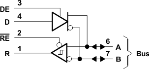
The SN65176B and SN75176B devices combine a 3-state differential line driver and a differential input line receiver, both of which operate from a single 5-V power supply. The driver and receiver have active-high and active-low enables, respectively, that can be connected together externally to function as a direction control. The driver differential outputs and the receiver differential inputs are connected internally to form differential input/output (I/O) bus ports that are designed to offer minimum loading to the bus when the driver is disabled or VCC = 0. These ports feature wide positive and negative common-mode voltage ranges, making the device suitable for party-line applications.
The driver is designed for up to 60 mA of sink or source current. The driver features positive and negative current limiting and thermal shutdown for protection from line-fault conditions. Thermal shutdown is designed to occur at a junction temperature of approximately 150°C. The receiver features a minimum input impedance of 12 kΩ, an input sensitivity of ±200 mV, and a typical input hysteresis of 50 mV.
| PART NUMBER | PACKAGE (PIN) | BODY SIZE (NOM) |
|---|---|---|
| SNx5176 | SOIC (8) | 4.90 mm × 3.91 mm |
| PDIP (8) | 9.81 mm × 6.35 mm | |
| SOP (8) | 6.20 mm × 5.30 mm |


