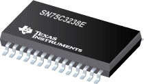

SN75C3238E是TI公司的一款无产品,SN75C3238E是具有 +/-15kV ESD (HBM) 保护的 3V 至 5.5V 多通道 RS-232 线路驱动器/接收器,本页介绍了SN75C3238E的产品说明、应用、特性等,并给出了与SN75C3238E相关的TI元器件型号供参考。
SN75C3238E - 具有 +/-15kV ESD (HBM) 保护的 3V 至 5.5V 多通道 RS-232 线路驱动器/接收器 - 无 - RS-232收发器 - TI公司(Texas Instruments,德州仪器)
- RS-232 Bus-Pin ESD Protection Exceeds ±15 kV Using Human-Body Model (HBM)
- Meet or Exceed the Requirements of TIA/EIA-232-F and ITU v.28 Standards
- Operate With 3-V to 5.5-V VCC Supply
- Operate up to 400 kbit/s
- Five Drivers and Three Receivers
- Auto-Powerdown Plus Feature Enables Flexible Power-Down Mode
- Low Standby Current . . . 1 µA Typical
- External Capacitors . . . 4 × 0.1 µF
- Accept 5-V Logic Input With 3.3-V Supply
- Always-Active Noninverting Receiver Output (ROUT1B)
- Alternative High-Speed Pin-Compatible Device (1 Mbit/s) for SNx5C3238
- ESD Protection for RS-232 Interface Pins
- ±15 kV - Human-Body Model (HBM)
- ±8 kV - IEC61000-4-2, Contact Discharge
- ±15 kV -IEC61000-4-2, Air-Gap Discharge
- APPLICATIONS
- Battery-Powered Systems
- PDAs
- Notebooks
- Subnotebooks
- Laptops
- Palmtop PCs
- Hand-Held Equipment
- Modems
- Printers
DESCRIPTION/ORDERING INFORMATION
The SN65C3238E and SN75C3238E consist of five line drivers, three line receivers, and a dual charge-pump circuit with ±15-kV ESD (HBM) protection on the driver output (DOUT) and receiver input (RIN) terminals. The devices meet the requirements of TIA/EIA-232-F and provide the electrical interface between notebook and subnotebook computer applications. The charge pump and four small external capacitors allow operation from a single 3-V to 5.5-V supply. In addition, the devices include an always-active noninverting output (ROUT1B), which allows applications using the ring indicator to transmit data while the device is powered down. These devices operate at data signaling rates up to 250 kbit/s and a maximum of 30-V/µs driver output slew rate.
Flexible control options for power management are featured when the serial port and driver inputs are inactive. The auto-powerdown plus feature functions when FORCEON is low and FORCEOFF is high. During this mode of operation, if the devices do not sense valid signal transitions on all receiver and driver inputs for approximately 30 s, the built-in charge pump and drivers are powered down, reducing the supply current to 1 µA. By disconnecting the serial port or placing the peripheral drivers off, auto-powerdown plus occurs if there is no activity in the logic levels for the driver inputs. Auto-powerdown plus can be disabled when FORCEON and FORCEOFF are high. With auto-powerdown plus enabled, the devices activate automatically when a valid signal is applied to any receiver or driver input. INVALID is high (valid data) if any receiver input voltage is greater than 2.7 V or less than -2.7 V, or has been between -0.3 V and 0.3 V for less than 30 µs. INVALID is low (invalid data) if all receiver input voltages are between -0.3 V and 0.3 V for more than 30 µs. Refer to Figure 5 for receiver input levels.


