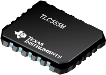

TLC555M是TI公司的一款无产品,TLC555M是低功耗 LinCMOS 定时器,本页介绍了TLC555M的产品说明、应用、特性等,并给出了与TLC555M相关的TI元器件型号供参考。
TLC555M - 低功耗 LinCMOS 定时器 - 无 - 定时器 - TI公司(Texas Instruments,德州仪器)
The TLC555 is a monolithic timing circuit fabricated using the TI LinCMOS™ process. The timer is fully compatible with CMOS, TTL, and MOS logic and operates at frequencies up to 2MHz. Because of its high input impedance, this device uses smaller timing capacitors than those used by the NE555. As a result, more accurate time delays and oscillations are possible. Power consumption is low across the full range of power supply voltage.
Like the NE555, the TLC555 has a trigger level equal to approximately one-third of the supply voltage and a threshold level equal to approximately two-thirds of the supply voltage. These levels can be altered by use of the control voltage terminal (CONT). When the trigger input (TRIG) falls below the trigger level, the flip-flop is set and the output goes high. If TRIG is above the trigger level and the threshold input (THRES) is above the threshold level, the flip-flop is reset and the output is low. The reset input (RESET) can override all other inputs and can be used to initiate a new timing cycle. If RESET is low, the flip-flop is reset and the output is low. Whenever the output is low, a low-impedance path is provided between the discharge terminal (DISCH) and GND. All unused inputs should be tied to an appropriate logic level to prevent false triggering.
While the CMOS output is capable of sinking over 100 mA and sourcing over 10 mA, the TLC555 exhibits greatly reduced supply-current spikes during output transitions. This minimizes the need for the large decoupling capacitors required by the NE555.
The TLC555C is characterized for operation from 0°C to 70°C. The TLC555I is characterized for operation from -40°C to 85°C. The TLC555Q is characterized for operation over the automotive temperature range of -40°C to 125°C. The TLC555M is characterized for operation over the full military temperature range of -55°C to 125°C.
- Very Low Power Consumption
- 1 mW Typ at VDD = 5 V
- Capable of Operation in Astable Mode
- CMOS Output Capable of Swinging Rail to Rail
- High Output-Current Capability
- Sink 100 mA Typ
- Source 10 mA Typ
- Output Fully Compatible With CMOS, TTL, and MOS
- Low Supply Current Reduces Spikes During Output Transitions
- Single-Supply Operation From 2 V to 15 V
- Functionally Interchangeable With the NE555; Has Same Pinout
- ESD Protection Exceeds 2000 V Per MIL-STD-883C, Method 3015.2
- Available in Q-Temp Automotive High Reliability Automotive Applications Configuration Control/Print Support Qualification to Automotive Standards
LinCMOS is a trademark of Texas Instruments.


