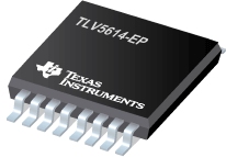

TLV5614-EP是TI公司的一款精密DAC(=<10MSPS)产品,TLV5614-EP是增强型产品四路 Dac,具有串行输入、可编程建立时间、低功耗、硬件或软件电源关闭功能,本页介绍了TLV5614-EP的产品说明、应用、特性等,并给出了与TLV5614-EP相关的TI元器件型号供参考。
TLV5614-EP - 增强型产品四路 Dac,具有串行输入、可编程建立时间、低功耗、硬件或软件电源关闭功能 - 精密DAC(=<10MSPS) - 数模转换器 - TI公司(Texas Instruments,德州仪器)
The TLV5614 is a quadruple 12-bit voltage output digital-to-analog converter (DAC) with a flexible four-wire serial interface. The four-wire serial interface allows glueless interface to TMS320™ DSP family, SPI™, QSPI™, and Microwire™ serial ports. The TLV5614 is programmed with a 16-bit serial word comprised of a DAC address, individual DAC control bits, and a 12-bit DAC value. The device has provision for two supplies - one digital supply for the serial interface (via pins DVDD and DGND), and one for the DACs, reference buffers, and output buffers (via pins AVDD and AGND). Each supply is independent of the other and can be any value between 2.7 V and 5.5 V. The dual supplies allow a typical application where the DAC is controlled via a microprocessor operating on a 3-V supply (also used on pins DVDD and DGND), with the DACs operating on a 5-V supply. The digital and analog supplies can be tied together.
The resistor string output voltage is buffered by a 2× gain rail-to-rail output buffer. The buffer features a Class AB output stage to improve stability and reduce settling time. A rail-to-rail output stage and a power-down mode makes it ideal for single-voltage, battery-based applications. The settling time of the DAC is programmable to allow the designer to optimize speed versus power dissipation. The settling time is chosen by the control bits within the 16-bit serial input string. A high-impedance buffer is integrated on the REFINAB and REFINCD terminals to reduce the need for a low source-impedance drive to the terminal. REFINAB and REFINCD allow DAC A and B to have a different reference voltage than DAC C and D.
The TLV5614 is implemented with a CMOS process and is available in a 16-terminal TSSOP package. The TLV5614M is characterized for operation from -55°C to 125°C.
- Controlled Baseline
- One Assembly
- One Test Site
- One Fabrication Site
- Extended Temperature Performance of -55°C to 125°C
- Enhanced Diminishing Manufacturing Sources (DMS) Support
- Enhanced Product-Change Notification
- Qualification Pedigree(1)
- Four 12-Bit Digital-to-Analog Converters (DACs)
- Programmable Settling Time of Either 3 µs or 9 µs (Typ)
- TMS320™ DSP Family, (Q)SPI™, and Microwire™ Compatible Serial Interface
- Internal Power-On Reset
- Low Power Consumption:
- 8 mW, Slow Mode - 5-V Supply
- 3.6 mW, Slow Mode - 3-V Supply
- Reference Input Buffer
- Voltage Output Range . . . 2× the Reference Input Voltage
- Monotonic Overtemperature
- Dual 2.7-V to 5.5-V Supply (Separate Digital and Analog Supplies)
- Hardware Power Down (10 nA)
- Software Power Down (10 nA)
- Simultaneous Update
- applications
- Battery-Powered Test Instruments
- Digital Offset and Gain Adjustment
- Industrial Process Controls
- Machine and Motion Control Devices
- Communications
- Arbitrary Waveform Generation
(1) Component qualification in accordance with JEDEC and industry standards to ensure reliable operation over an extended temperature range. This includes, but is not limited to, Highly Accelerated Stress Test (HAST) or biased 85/85, temperature cycle, autoclave or unbiased HAST, electromigration, bond intermetallic life, and mold compound life. Such qualification testing should not be viewed as justifying use of this component beyond specified performance and environmental limits. TMS320 is a trademark of Texas Instruments. All other trademarks are the property of their respective owners.


