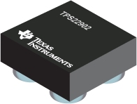

TPS22902是TI公司的一款配电与蓄电产品,TPS22902是具有快速输出放电功能的 3.6V,0.5A,78mΩ 负载开关,本页介绍了TPS22902的产品说明、应用、特性等,并给出了与TPS22902相关的TI元器件型号供参考。
TPS22902 - 具有快速输出放电功能的 3.6V,0.5A,78mΩ 负载开关 - 配电与蓄电 - 集成负载开关 - TI公司(Texas Instruments,德州仪器)
- Integrated P-Channel Load Switch
- Low Input Voltage: 1 V to 3.6 V
- ON-Resistance (Typical Values)
- rON = 78 mΩ at VIN = 3.6 V
- rON = 93 mΩ at VIN = 2.5 V
- rON = 109 mΩ at VIN = 1.8 V
- rON = 146 mΩ at VIN = 1.2 V
- 500 mA Maximum Continuous Switch Current
- Quiescent Current: 82 nA at 1.8 V
- Shutdown Current: 44 nA at 1.8 V
- Low Control Input Thresholds Enable Use of 1.2-V, 1.8-V, 2.5-V, and 3.3-V Logic
- Controlled Slew Rate to Avoid Inrush Currents
- tr = 40 μs at VIN = 1.8 V (TPS22901/2)
- tr = 220 μs at VIN = 1.8 V (TPS22902B)
- Quick Output Discharge (TPS22902/2B)
- ESD Performance Tested Per JESD 22
- 2000-V Human Body Model (A114-B, Class II)
- 1000-V Charged-Device Model (C101)
- Four-Pin Wafer-Chip-Scale DSBGA Package
- 0.8-mm × 0.8-mm, 0.4-mm Pitch, 0.5-mm Height (YFP)
- Personal Digital Assistants (PDAs)
- Cellular Phones
- GPS Devices
- MP3 Players
- Digital Cameras
- Peripheral Ports
- Portable Instrumentation
- RF Modules
The TPS22901, TPS22902, and TPS22902B are small, low ON-resistance (rON) load switches with a controlled turnon. These devices contain a P-channel MOSFET that operates over an input voltage range of 1.0 V to 3.6 V. The switch is controlled by an on/off input (ON), which can interface directly with low-voltage control signals. In the TPS22902 and TPS22902B, an 88-Ω on-chip load resistor is added for output quick discharge when the switch is turned off.
The TPS22901, TPS22902, and TPS22902B are available in a space-saving 4-pin DSBGA (YFP) with 0.4-mm pitch. These devices are characterized for operation over the free-air temperature range of –40°C to 85°C.
| PART NUMBER | PACKAGE | BODY SIZE (NOM) |
|---|---|---|
| TPS22901 | DSBGA (4) | 0.80 mm × 0.80 mm |
| TPS22902 | ||
| TPS22902B |


