


TPS53317A是TI公司的一款无产品,TPS53317A是用于 DDR 存储器终端的 6A 输出 D-CAP+ 模式同步降压集成 FET 转换器,本页介绍了TPS53317A的产品说明、应用、特性等,并给出了与TPS53317A相关的TI元器件型号供参考。
TPS53317A - 用于 DDR 存储器终端的 6A 输出 D-CAP+ 模式同步降压集成 FET 转换器 - 无 - DDR存储器电源终端 - TI公司(Texas Instruments,德州仪器)
- TI-Proprietary Integrated MOSFET and Packaging Technology
- Supports DDR Memory Termination with up to 6-A Continuous Output Source or Sink Current
- External Tracking
- Minimum External Components Count
- 0.9-V to 6-V Conversion Voltage
- D-CAP+™ Mode Architecture
- Supports All MLCC Output Capacitors and SP/POSCAP
- Selectable SKIP Mode or Forced CCM
- Optimized Efficiency at Light and Heavy Loads
- Selectable 600-kHz or 1-MHz Switching Frequency
- Selectable Overcurrent Limit (OCL)
- Overvoltage, Over-Temperature and Hiccup Undervoltage Protection
- Adjustable Output Voltage from 0.45 V to 2 V
- 3.5 mm × 4 mm, 20-Pin, VQFN Package
- Memory Termination Regulator for DDR, DDR2, DDR3, DDR3L, and DDR4
- VTT Termination
- Low-Voltage Applications for 0.9-V to 6-V Input Rails
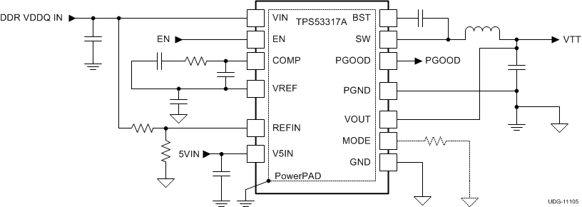
The TPS53317A device is a FET-integrated synchronous buck regulator designed mainly for DDR termination. It can provide a regulated output at ½ VDDQ with both sink and source capability. The TPS53317A device employs D-CAP+ mode operation that provides ease of use, low external component count and fast transient response. The device can also be used for other point-of-load (POL) regulation applications requiring up to 6 A. In addition, the device supports full, 6-A, output sinking current capability with tight voltage regulation.
The device features two switching frequency settings (600 kHz and 1 MHz), integrated droop support, external tracking capability, pre-bias startup, output soft discharge, integrated bootstrap switch, power good function, V5IN pin UVLO protection, and supports both ceramic and SP/POSCAP capacitors. It supports input voltages up to 6.0 V, and output voltages adjustable from 0.45 V to 2.0 V.
The TPS53317A device is available in the 3.5 mm × 4 mm, 20-pin, VQFN package (Green RoHs compliant and Pb free) with TI proprietary Integrated MOSFET and packaging technology and is specified from –40°C to 85°C.
| PART NUMBER | PACKAGE | BODY SIZE (NOM) |
|---|---|---|
| TPS53317A | VQFN (20) | 3.50 mm × 4.00 mm |

