
TPS61170是TI公司的一款转换器(集成开关)产品,TPS61170是采用了 2x2mm QFN 封装的 1.2A 开关、高压升压转换器,本页介绍了TPS61170的产品说明、应用、特性等,并给出了与TPS61170相关的TI元器件型号供参考。
TPS61170 - 采用了 2x2mm QFN 封装的 1.2A 开关、高压升压转换器 - 转换器(集成开关) - DC/DC开关稳压器 - TI公司(Texas Instruments,德州仪器)
- 3-V to 18-V Input Voltage Range
- High Output Voltage: Up to 38 V
- 1.2-A Integrated Switch
- 1.2-MHz Fixed Switching Frequency
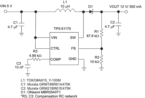
- 12 V at 300 mA and 24 V at 150 mA From 5-V Input (Typical)
- Up to 93% Efficiency
- On-The-Fly Output Voltage Reprogramming
- Skip-Switching Cycle for Output Regulation at Light Load
- Built-in Soft Start
- 6-Pin, 2-mm × 2-mm QFN Package
- 5-V to 12-V and 24-V, 12-V to 24-V Boost Converter
- Buck Boost Regulation Using SEPIC Topology
- ADSL Modems
The TPS61170 is a monolithic, high-voltage switching regulator with integrated 1.2-A, 40-V power MOSFET. The device can be configured in several standard switching-regulator topologies, including boost and SEPIC. The device has a wide input-voltage range to support applications with input voltage from multicell batteries or regulated 5-V, 12-V power rails.
The TPS61170 operates at a 1.2-MHz switching frequency, allowing the use of low-profile inductors and low-value ceramic input and output capacitors. External loop compensation components give the user flexibility to optimize loop compensation and transient response. The device has built-in protection features, such as pulse-by-pulse overcurrent limit, soft start, and thermal shutdown.
The FB pin regulates to a reference voltage of 1.229 V. The reference voltage can be lowered using a 1-wire digital interface (Easyscale™ protocol) through the CTRL pin. Alternatively, a pulse width-modulation (PWM) signal can be applied to the CTRL pin. The duty cycle of the signal reduces the feedback reference voltage proportionally.
The TPS61170 is available in a 6-pin 2-mm × 2-mm QFN package, allowing a compact power-supply solution.
| PART NUMBER | PACKAGE | BODY SIZE (NOM) |
|---|---|---|
| TPS61170 | VSON (6) | 2.00 mm x 2.00 mm |


