
TPS63051是TI公司的一款转换器(集成开关)产品,TPS63051是小型单电感器降压/升压转换器,本页介绍了TPS63051的产品说明、应用、特性等,并给出了与TPS63051相关的TI元器件型号供参考。
TPS63051 - 小型单电感器降压/升压转换器 - 转换器(集成开关) - DC/DC开关稳压器 - TI公司(Texas Instruments,德州仪器)
- Real Buck or Boost with Seamless Transition Between Buck and Boost Mode
- 2.5 V to 5.5 V Input Voltage Range
- 0.5-A Continuous Output Current: VIN ≥ 2.5 V, VOUT = 3.3 V
- Adjustable and Fixed Output Voltage Version
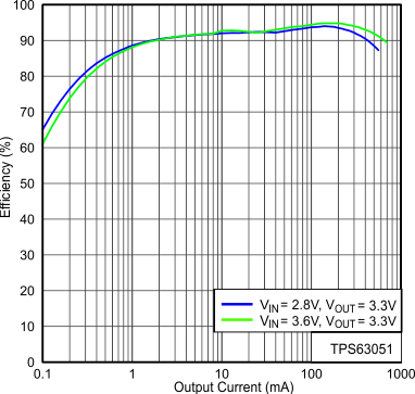
- Efficiency > 90% in Boost Mode and > 95% in Buck Mode
- 2.5-MHz Typical Switching Frequency
- Adjustable Average Input Current Limit
- Adjustable Soft-Start Time
- Device Quiescent Current < 60 μA
- Automatic Power Save Mode or Forced PWM Mode
- Load Disconnect During Shutdown
- Overtemperature Protection
- Small 1.6mm x 1.2mm, 12-pin WCSP and 2.5mm x 2.5mm 12-pin HotRod™ QFN package
- Cellular and Smart Phones
- Tablets PC
- PC and Smart Phone Accessories
- Battery Powered Applications
- Smart Grid/Smart Meter
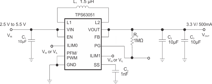
The TPS6305x family of devices is a high efficiency, low quiescent-current buck-boost converter, suitable for applications where the input voltage is higher or lower than the output.
Continuous output current can go as high as 500 mA in boost mode and as high as 1 A in buck mode. The maximum average current in the switches is limited to a typical value of 1 A. The TPS6305x family of devices regulate the output voltage over the complete input voltage range by automatically switching between buck or boost mode depending on the input voltage, ensuring seamless transition between modes.
The buck-boost converter is based on a fixed-frequency, pulse-width-modulation (PWM) controller using synchronous rectification to obtain the highest efficiency. At low load currents, the converter enters Power Save Mode to maintain high efficiency over the complete load current range.
The PFM/PWM pin allows the user to select between automatic-PFM/PWM mode operation and forced-PWM operation. During PWM mode a fixed-frequency of typically 2.5 MHz is used. The output voltage is programmable using an external resistor divider, or is fixed internally on the chip. The converter can be disabled to minimize battery drain. During shutdown, the load is disconnected from the battery. The device is packaged in a 12-pin DSBGA and in a 12-pin HotRod package.
| PART NUMBER | PACKAGE | BODY SIZE (NOM) |
|---|---|---|
| TPS63050 | DSBGA (12) | 1.56mm x 1.16mm |
| TPS63051 | VQFN (12) | 2.50mm × 2.50mm |


