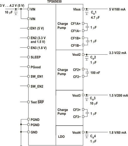

TPS65030是TI公司的一款无产品,TPS65030是面向 USB-OTG 的芯片级封装电源管理 IC,具有 3 个电荷泵和 1 个 LDO,本页介绍了TPS65030的产品说明、应用、特性等,并给出了与TPS65030相关的TI元器件型号供参考。
TPS65030 - 面向 USB-OTG 的芯片级封装电源管理 IC,具有 3 个电荷泵和 1 个 LDO - 无 - 电源管理多通道IC(PMIC)解决方案 - TI公司(Texas Instruments,德州仪器)
- Four Regulated Output Voltages With 3% Tolerance
- Fractional Charge Pump for 5 V, 100 mA
- Fractional Charge Pump for 1.5 V, 200 mA
- Doubling Charge Pump With LDO Mode for 3.3 V, 22 mA
- LDO for 1.8 V, 60 mA
- Switching Frequency 1 MHz
- 3-V to 5-V Operating Input Voltage Range at VCC Pin
- Sleep Mode Sets Vout2 and Vout3 Into LDO Mode
- Sleep Mode Reduces Quiescent Current of Vout2, Vout3, and Vout4 to 8-μA Each
- Internal Bus Switch
- Vbus Comparator
- Internal Soft Start Limits Inrush Current
- Low Input Current Ripple and Low EMI
- Overcurrent and Overtemperature Protected
- Undervoltage Lockout With Hysteresis
- Ultra-Small 2.50-mm × 2.70-mm Chip Scale Package Applications
- Power Supply for USB OTG for:
- Cellular Phones
- Smart Phones
- PDAs
- Handheld PCs
- Digital Cameras
- Camcorders
The TPS65030 device contains three charge pumps and one LDO to generate all supply voltages necessary for a USB On-The-Go (OTG) implementation using TUSB6010. The charge pumps are optimized for a single Li-Ion cell input or for 5 V from the USB bus. The input voltage range is 3 V to 5 V for the battery voltage. High efficiency is achieved by using fractional conversion techniques for the charge pumps in combination with a power saving sleep mode. The current-controlled charge pumps ensure low input current ripple and low EMI. Small sized external ceramic capacitors are required to build a complete power-supply solution. To reduce board space to a minimum, the device switches at 1-MHz operating frequency and is available in a small 25-ball chip scale package (YZK).
| PART NUMBER | PACKAGE | BODY SIZE (MAX) |
|---|---|---|
| TPS65030 | DSBGA (25) | 2.51 mm × 2.70 mm |


