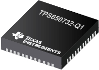

TPS650732-Q1是TI公司的一款无产品,TPS650732-Q1是采用 6mm x 6mm QFN 封装的汽车类 5 通道电源管理 IC (PMIC),具有 3 个 DC/DC 和 2 个 LDO,本页介绍了TPS650732-Q1的产品说明、应用、特性等,并给出了与TPS650732-Q1相关的TI元器件型号供参考。
TPS650732-Q1 - 采用 6mm x 6mm QFN 封装的汽车类 5 通道电源管理 IC (PMIC),具有 3 个 DC/DC 和 2 个 LDO - 无 - 电源管理多通道IC(PMIC)解决方案 - TI公司(Texas Instruments,德州仪器)
The TPS6507x are single chip Power Management ICs for portable applications consisting of a battery charger with power path management for a single Li-Ion or Li-Polymer cell. The charger can either be supplied by a USB port on pin USB or by a dc voltage from a wall adapter connected to pin AC. Three highly efficient 2.25MHz step-down converters are targeted at providing the core voltage, memory and I/O voltage in a processor based system. The step-down converters enter a low power mode at light load for maximum efficiency across the widest possible range of load currents. For low noise applications the devices can be forced into fixed frequency PWM using the I2C interface. The step-down converters allow the use of small inductors and capacitors to achieve a small solution size. The TPS6507x also integrate two general purpose LDOs for an output current of 200mA. These LDOs can be used to power an SD-card interface and an always-on rail, but can be used for other purposes as well. Each LDO operates with an input voltage range between 1.8V and 6.3V allowing them to be supplied from one of the step-down converters or directly from the main battery. An inductive boost converter with two programmable current sinks power two strings of white LEDs.
The TPS6507x come in a 48-pin leadless package (6mm × 6mm QFN) with a 0.4mm pitch.
- Qualified for Automotive Applications
- Charger/Power Path Management:
- 2A Output Current on the Power Path
- Linear Charger; 1.5A Maximum Charge Current
- 100mA/500mA/ 800mA/1300mA Current Limit From USB Input
- Thermal Regulation, Safety Timers
- Temperature Sense Input
- 3 Step-Down Converters:
- 2.35MHz Fixed Frequency Operation
- Up to 1.5A of Output Current
- Adjustable or Fixed Output Voltage
- VIN Range From 2.8V to 6.3V
- Power Save Mode at Light Load Current
- Output Voltage Accuracy in PWM Mode ±1.5%
- Typical 19µA Quiescent Current per Converter
- 100% Duty Cycle for Lowest Dropout
- LDOs:
- Fixed Output Voltage
- Dynamic Voltage Scaling on LDO2
- 20µA Quiescent Current
- 200mA Maximum Output Current
- VIN Range From 1.8V to 6.3V
- wLED Boost Converter:
- Internal Dimming Using I2C
- Up to 2 × 10 LEDs
- Up to 25mA per String With Internal Current Sink
- I2C Interface
- 10 Bit A/D Converter
- Touch Screen Interface
- Undervoltage Lockout and Battery Fault Comparator
- APPLICATIONS
- Portable Navigation Systems
- Low-Power DSP Supply


