
TPS65130是TI公司的一款转换器(集成开关)产品,TPS65130是具有正负(双路)输出的 800mA 升压电流,用于 OLED 和 CCD 传感器,24 QFN,本页介绍了TPS65130的产品说明、应用、特性等,并给出了与TPS65130相关的TI元器件型号供参考。
TPS65130 - 具有正负(双路)输出的 800mA 升压电流,用于 OLED 和 CCD 传感器,24 QFN - 转换器(集成开关) - DC/DC开关稳压器 - TI公司(Texas Instruments,德州仪器)
- Dual Adjustable Output Voltages Up to 15 V and Down to –15 V
- 800-mA Typical Switch Current Limit at Boost and Inverter Main Switches at TPS65130
- 2-A Typical Switch Current Limit at Boost and Inverter Main Switches at TPS65131
- Up to 89% Efficiency at Positive Output Voltage Rail
- Up to 81% Efficiency at Negative Output Voltage Rail
- Power-Save Mode for High Efficiency at Low Load Currents
- Independent Enable Inputs for Power-Up and Power-Down Sequencing
- Control Output for External PFET to Support Completely Disconnecting the Battery
- 2.7-V to 5.5-V Input Voltage Range
- Minimum 1.25-MHz Fixed Frequency PWM Operation
- Thermal Shutdown
- Overvoltage Protection on Both Outputs
- 1-µA Shutdown Current
- Small 4-mm x 4-mm VQFN-24 Package (RGE)
- Small to Medium Size OLED Displays
- (TFT) LCD and CCD Bias Supply
- PDAs, Pocket PCs, Smartphones
- Digital Cameras
- Camcorders
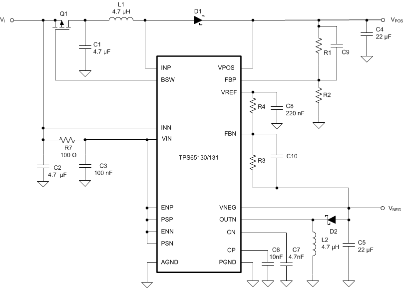
The TPS6513x is dual-output DC-DC converter generating a positive output voltage up to 15 V and a negative output voltage down to –15 V with output currents in a 200-mA range in typical applications, depending on input voltage to output voltage ratio. With a total efficiency up to 85%, the device is ideal for portable battery-powered equipment. The input voltage range of 2.7 V to 5.5 V allows the TPS65130/1 to be directly powered from a Li-ion battery, from 3 cells NiMH/NiCd or alkaline batteries. The TPS6513x comes in a small 4-mm × 4-mm VQFN-24 package. Together with a minimum switching frequency of 1.25 MHz, the device enables designing small power supply applications because it requires only a few small external components.
The converter operates with a fixed frequency PWM control topology and, if power-save mode is enabled, it uses a pulse-skipping mode at light-load currents. It operates with only 500-µA device quiescent current. Independent enable pins allow power-up and power-down sequencing for both outputs. The device has an internal current limit overvoltage protection and a thermal shutdown for highest reliability under fault conditions.
| PART NUMBER | PACKAGE | BODY SIZE (NOM) |
|---|---|---|
| TPS65130 | VQFN (24) | 4.00 mm × 4.00 mm |
| TPS65131 | VQFN (24) | 4.00 mm × 4.00 mm |


