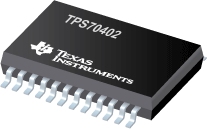

TPS70402是TI公司的一款多通道LDO产品,TPS70402是双路输出 1A/2A 低压降 (LDO),具有双路启用功能和用于分压系统的 SVS,本页介绍了TPS70402的产品说明、应用、特性等,并给出了与TPS70402相关的TI元器件型号供参考。
TPS70402 - 双路输出 1A/2A 低压降 (LDO),具有双路启用功能和用于分压系统的 SVS - 多通道LDO - 线性稳压器(LDO) - TI公司(Texas Instruments,德州仪器)
The TPS704xx family of devices consists of dual-output, low-dropout voltage regulators with integrated SVS (RESET, POR, or power on reset) and power good (PG) functions. These devices are capable of supplying 1 A and 2 A by regulator 1 and regulator 2 respectively. Quiescent current is typically 185 µA at full load. Differentiated features, such as accuracy, fast transient response, SVS supervisory circuit (power on reset), manual reset input, and independent enable functions provide a complete system solution.
The TPS704xx family of voltage regulators offers very low dropout voltage and dual outputs. These devices have extremely low noise output performance without using any added filter bypass capacitors and are designed to have a fast transient response and be stable with 47-µF low ESR capacitors.
These devices have fixed 3.3-V/2.5-V, 3.3-V/1.8-V, 3.3-V/1.5-V, 3.3-V/1.2-V, and adjustable voltage options. Regulator 1 can support up to 1 A, and regulator 2 can support up to 2 A. Separate voltage inputs allow the designer to configure the source power.
Because the PMOS device behaves as a low-value resistor, the dropout voltage is very low (typically 160 mV on regulator 1) and is directly proportional to the output current. Additionally, since the PMOS pass element is a voltage-driven device, the quiescent current is very low and independent of output loading (maximum of 250 µA over the full range of output current and full range of temperature). This LDO family also features a sleep mode; applying a high signal to EN1 or EN2 (enable) shuts down regulator 1 or regulator 2, respectively. When a high signal is applied to both EN1 and EN2, both regulators enter sleep mode, thereby reducing the input current to 2 µA at TJ = +25°C.
For each regulator, there is an internal discharge transistor to discharge the output capacitor when the regulator is turned off (disabled).
The PG1 pin reports the voltage condition at VOUT1. The PG1 pin can be used to implement a SVS (RESET, POR, or power on reset) for the circuitry supplied by regulator 1. The PG2 pin reports the voltage conditions at VOUT2. The PG2 pin can be used to implement a SVS (power on reset) for the circuitry supplied by regulator 2.
The TPS704xx features a RESET (SVS, POR, or power on reset). RESET is an active low, open drain output and requires a pull-up resistor for normal operation. When pulled up, RESET goes into a high impedance state (that is, logic high) after a 120-ms delay when both of the following conditions are met. First, VIN1 must be above the undervoltage condition. Second, the manual reset (MR) pin must be in a high impedance state. To monitor VOUT1, the PG1 output pin can be connected to MR. To monitor VOUT2, the PG2 output pin can be connected to MR. RESET can be used to drive power on reset or a low-battery indicator. If RESET is not used, it can be left floating.
Internal bias voltages are powered by VIN1 and require 2.7 V for full functionality. Each regulator input has an undervoltage lockout circuit that prevents each output from turning on until the respective input reaches 2.5 V.
- Dual Output Voltages for Split-Supply Applications
- Independent Enable Functions (See Part Number TPS703xx for Sequenced Outputs)
- Output Current Range of 1 A on Regulator 1 and 2 A on Regulator 2
- Fast Transient Response
- Voltage Options: 3.3-V/2.5-V, 3.3-V/1.8-V, 3.3-V/1.5-V, 3.3-V/1.2-V, and Dual Adjustable Outputs
- Open Drain Power-On Reset with 120-ms Delay
- Open Drain Power Good for Regulator 1 and Regulator 2
- Ultralow 185µA (typ) Quiescent Current
- 2µA Input Current During Standby
- Low Noise: 78µVRMS Without Bypass Capacitor
- Quick Output Capacitor Discharge Feature
- One Manual Reset Input
- 2% Accuracy Over Load and Temperature
- Undervoltage Lockout (UVLO) Feature
- 24-Pin PowerPAD™ TSSOP Package
- Thermal Shutdown Protection
PowerPAD is a trademark of Texas Instruments. All other trademarks are the property of their respective owners.


