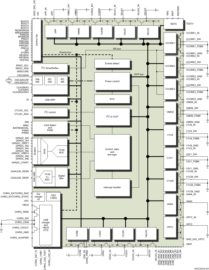

TWL6030是TI公司的一款TI芯片产品,TWL6030是具有开关模式充电器的全集成电源管理 IC (PMIC),本页介绍了TWL6030的产品说明、应用、特性等,并给出了与TWL6030相关的TI元器件型号供参考。
TWL6030 - 具有开关模式充电器的全集成电源管理 IC (PMIC) - TI芯片 - 电源管理多通道IC(PMIC)解决方案 - TI公司(Texas Instruments,德州仪器)
- Seven Highly Efficient 6-MHz Buck Converters
- Two 0.6 to 2.1 V at 1.5 A (up to 2.0 A with some Limitations)
- Five 0.6 to 2.1 V at 0.8 A (up to 1.0 A with some Limitations)
- 11 General-Purpose LDOs
- Six 1.0 to 3.3 V at 0.2 A with Battery or Preregulated Supply (One can be used as a Vibrator Driver)
- One 1.0 to 3.3 V at 50 mA with Battery or Preregulated Supply
- One Low Noise 1.0 to 3.3 V at 50 mA with Battery or Preregulated Supply
- 3.3 V at 35 mA USB LDO
- One LDO for TWL6030 Internal Use
- One LDO for Internal and External Use
- USB OTG Module
- Backup Battery Charger
- 10-Bit ADC with 17 Input Channels
- 13-Bit Coulomb Counter with Four Programmable Integration Periods
- Low-Power Consumption
- 5 µA in Backup Mode
- 20 µA in Wait-on Mode
- 110 µA in Deep Sleep, with Two DC-DC Converters Active
- RTC with Alarm Wake-up Mechanism
- SIM and MMC Card Detections
- Two Digital PWM Outputs
- Thermal Monitoring
- High-Temperature Warning
- Thermal Shutdown
- Control
- Configurable Power-up and Power-down Sequences (OTP Memory)
- Three Output Signals that can be Included in the Start-up Sequence
- Two I2C Interfaces
- All Resources Configurable by I2C
- Clock Management
- Battery Charger 1.5 A
- Charger for Single-Cell Li-Ion and Li-Polymer Battery Packs
- Switched-Mode Charger with Integrated Power FET for up to 1.5-A Current
- High-Accuracy Voltage and Current Regulation
- Safety Timer and Reset Control
- Thermal Regulation Protection
- Input/Output Overvoltage Protection
- Charging Indicator LED Driver
- Boost Mode Operation for USB OTG
- Compliant with:
- USB 2.0
- OTG and EH 2.0
- YD/T 1591-2006
- USB Battery Charging 1.2
- Japanese Battery Charging Requirements (JEITA)
- Package: 7 mm x 7 mm 187-Pin nFBGA
32-kHz Output
- Mobile Phones and Smart Phones
- Gaming Handsets
- Portable Media Players
- Portable Navigation Systems
- Handheld Devices
- Tablets
The TWL6030 device is an integrated power-management integrated circuit (IC) for applications powered by a rechargeable battery. The device provides seven configurable step-down converters with up to 2.0-A capability for memory, processor core, I/O, auxiliary, preregulation for LDOs, and so forth. The device also contains 11 LDO regulators that can be supplied from a battery or a preregulated supply. The power-up and power-down controller is configurable and can support any power-up and power-down sequences (programmed in OTP memory). The real-time clock (RTC) provides a 32-kHz output buffer, second, minute, hour, day, month, year information, and alarm wake up. The TWL6030 device supports 32-kHz clock generation based on a crystal oscillator. The device integrates a switched-mode charger allowing faster battery charge, higher efficiency, and less power dissipation.
The TWL6030 device generates power supplies for OMAP™ 4 processors and operates together with the TWL6040 device, which includes all audio and related detection features. For audio IC parameters, see the TWL6040 data sheet. The TWL6030 device is available in an nFBGA package, 7.0 mm x 7.0 mm, with a 0.4-mm ball pitch.
| PART NAME | PACKAGE | BODY SIZE |
|---|---|---|
| TWL6030 | FC/CSP [FCBGA] (187) | 7.00 mm x 7.00 mm |


