
UCC27201A是TI公司的一款半桥驱动器产品,UCC27201A是120V 升压 3A 峰值电流的高频高侧/低侧驱动器,本页介绍了UCC27201A的产品说明、应用、特性等,并给出了与UCC27201A相关的TI元器件型号供参考。
UCC27201A - 120V 升压 3A 峰值电流的高频高侧/低侧驱动器 - 半桥驱动器 - MOSFET和IGBT栅极驱动器 - TI公司(Texas Instruments,德州仪器)
- Drives Two N-Channel MOSFETs in High-Side and Low-Side Configuration
- Negative Voltage Handling on HS (–18V)
- Maximum Boot Voltage 120 V
- Maximum VDD Voltage 20 V
- On-Chip 0.65-V VF, 0.6-Ω RD Bootstrap Diode
- Greater than 1 MHz of Operation
- 20-ns Propagation Delay Times
- 3-A Sink, 3-A Source Output Currents
- 8-ns Rise/7-ns Fall Time with 1000-pF Load
- 1-ns Delay Matching
- Undervoltage Lockout for High-Side and Low-Side Driver
- Offered in 8-Pin SOIC (D), PowerPAD™ SOIC-8 (DDA), SON-8 (DRM), SON-9 (DRC) and SON-10 (DPR) Packages
- Specified from –40°C to 140°C
- Power Supplies for Telecom, Datacom, and Merchant Markets
- Half-Bridge Applications and Full-Bridge Converters
- Isolated Bus Architecture
- Two-Switch Forward Converters
- Active-Clamp Forward Converters
- High-Voltage Synchronous-Buck Converters
- Class-D Audio Amplifiers
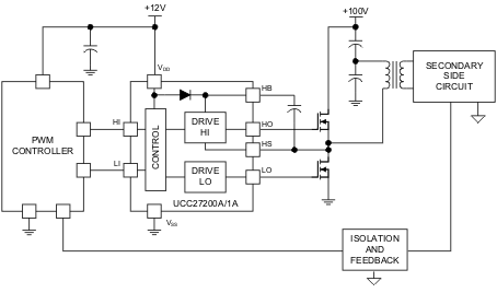
The UCC2720xA family of high-frequency N-channel MOSFET drivers include a 120-V bootstrap diode and high-side/low-side driver with independent inputs for maximum control flexibility. This allows for N-channel MOSFET control in half-bridge, full-bridge, two-switch forward and active clamp forward converters. The low-side and the high-side gate drivers are independently controlled and matched to 1-ns between the turn-on and turn-off of each other. The UCC2720xA are based on the popular UCC27200/1 drivers, but offer some enhancements. In order to improve performance in noisy power supply environments the UCC2720xA has an enhanced ESD input structure and also has the ability to withstand a maximum of –18 V on its HS pin.
An on-chip bootstrap diode eliminates the external discrete diodes. Under-voltage lockout is provided for both the high-side and the low-side drivers forcing the outputs low if the drive voltage is below the specified threshold.
Two versions of the UCC27200A are offered. The UCC27200A has high-noise immune CMOS input thresholds while the UCC27201A has TTL-compatible thresholds.
Both devices are offered in an 8-pin SOIC (D), PowerPad SOIC-8 (DDA), SON-8 (DRM) package, a 9-pin SON-9 (DRC) package and a 10-pin SON-10 (DPR) package.
| PART NUMBER | PACKAGE | BODY SIZE (NOM) |
|---|---|---|
| UCC27200A, UCC27201A | SOIC (8) | 4.90 mm × 3.91 mm |
| HSOP (8) | 4.89 mm × 3.90 mm | |
| VSON (9) | 3.00 mm × 3.00 mm | |
| VSON (8) | 4.00 mm × 4.00 mm | |
| UCC27201A | WSON (10) | 4.00 mm × 4.00 mm |


